
Starting with a Hardware Engineer’s Basic Skill
Soldering connects electronic components to printed circuit boards (PCBs). This step is vital for PCBA manufacturing. You see soldering everywhere, from manual soldering in labs to prototype validation and mass production in PCBA factories. In automated production, reflow soldering and wave soldering are the two most common and essential processes. For PCBA suppliers, choosing the right soldering process directly affects product yield, delivery time, and manufacturing cost.
This article compares reflow soldering and wave soldering based on IPC and other standards. It covers principles, processes, parameters, and quality control. PCB designers and PCBA purchasing managers will get a practical and in-depth selection guide.
1. Reflow Soldering: Precise Heating for SMT Assembly
Reflow soldering is the mainstream process for surface mount technology (SMT). Its core logic is “solder exists first, then heat melts it.” You print solder paste (with flux) on PCB pads using a stencil. A pick-and-place machine mounts surface mount devices (SMDs) onto the paste. Then the whole board goes into a reflow oven. A controlled temperature profile melts the paste and forms reliable solder joints.
1.1 Four Temperature Zones with Precise Control
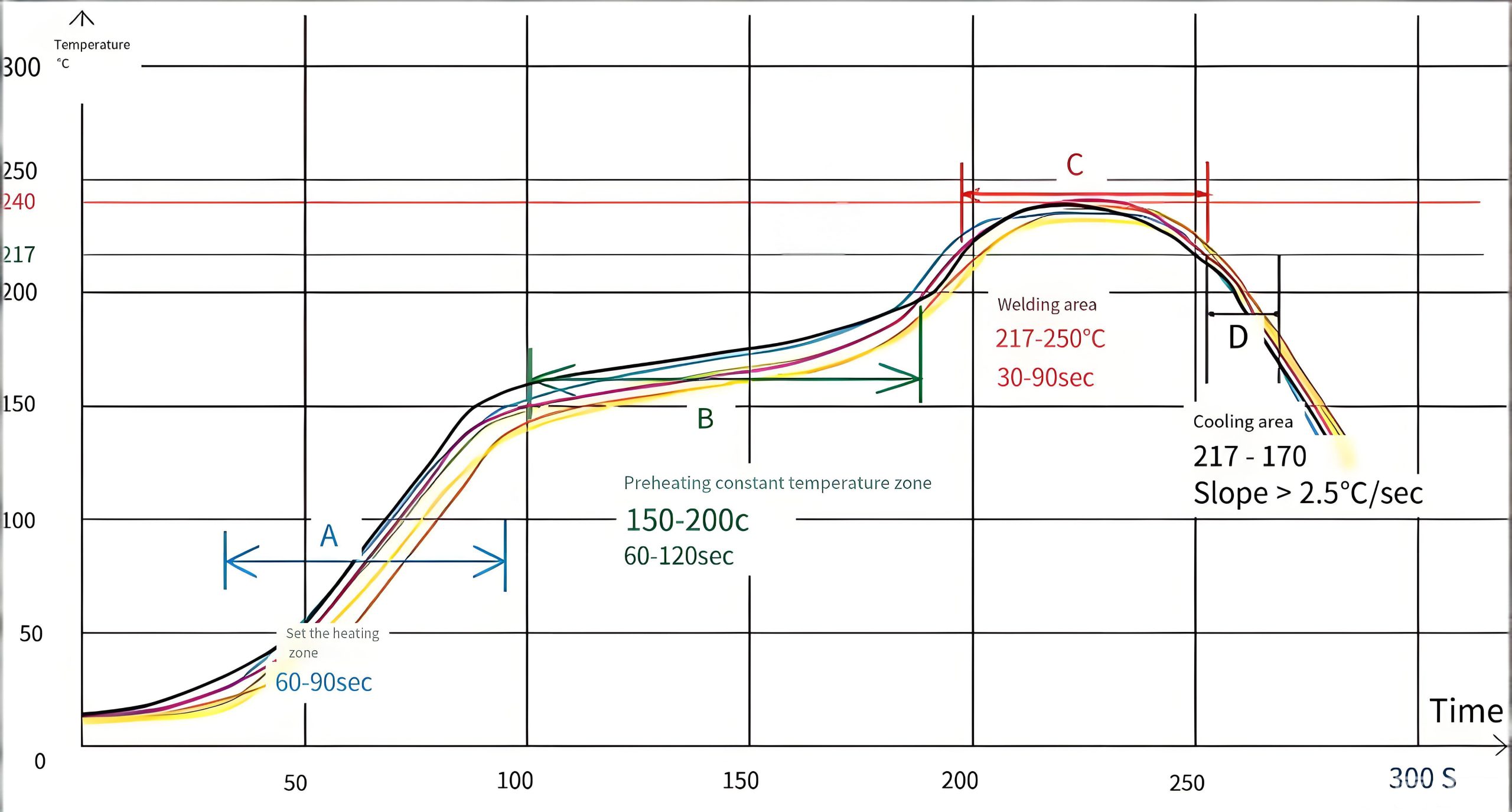
According to IPC-2221, a typical reflow profile has four key stages.
- Preheat Zone: Temperature rises from room temperature to 150-160°C. The ramp rate stays between 1-3°C/s. This allows solvents in the paste to evaporate slowly, removing bubbles and preventing solder splatter. Thick boards need longer preheat (about 3-4 minutes). Thin boards need about 1-2 minutes.
- Soak Zone (Activation Zone): Temperature holds at 150-180°C for 60-120 seconds. The flux activates fully and removes oxides from pads and component leads.
- Reflow Zone (Peak Zone): Temperature goes above the solder melting point. Lead-free solder (like SAC305) melts at about 217°C. Peak temperature reaches 235-250°C for 10-20 seconds. This melts the solder and allows wetting on pads and leads, forming an intermetallic compound (IMC). Leaded solder (Sn63Pb37) melts at about 183°C, with a peak of 210-220°C.
- Cooling Zone: The board cools down quickly at 2-4°C/s. The solder solidifies into a strong joint. If cooling is too fast (over 6°C/s), thermal stress increases crack risk by three times. If cooling is too slow, grain structure becomes coarse, lowering joint strength.
1.2 Key Quality Control Metrics
Defects from reflow soldering cause over 60% of all PCBA failures. According to IPC-A-610G, you must meet these quality requirements: wetting angle ≤25°, IMC thickness between 0.8-1.5μm, and void ratio ≤5%. Industry data shows that with precise process control, SMT lines can reduce defect rates from 3.2% to below 0.05%.
2. Wave Soldering: Tin Wave Wetting for Through-Hole Assembly
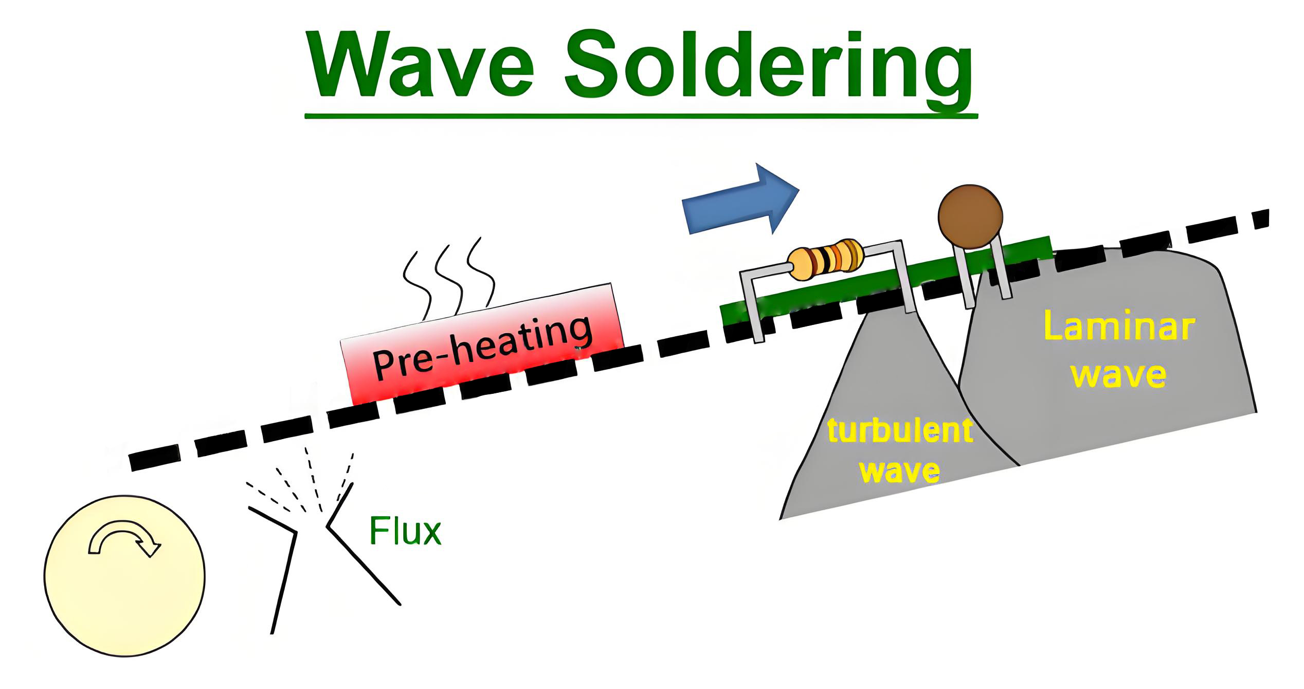
Wave soldering mainly serves through-hole technology (THT) and mixed assemblies with through-hole components. Its core logic is “solder supplies continuously, then wets and solidifies.” A pump creates a wave of molten solder in a tank. The PCB, with components inserted, passes over this wave at a fixed angle. The liquid solder wets the component leads and PCB pads. After cooling, the joints form.
2.1 Quantitative Control of Key Process Parameters
Proper parameter settings determine wave soldering quality. Reliable industry data shows that a ±5°C variation in solder temperature increases cold joint rates from 1% to 8%. A 0.2 m/min variation in conveyor speed raises bridging defects by 5%.
- Solder Temperature: For lead-free SAC305, standard temperature is 250-255°C. High-temperature lead-free SAC405 runs at 260-265°C. Low-temperature lead-free Sn42Bi58 needs only 180-190°C, suitable for heat-sensitive components.
- Conveyor Speed: The standard range is 1-1.5 m/min, giving 3-5 seconds of contact time. Contact time = wave length ÷ conveyor speed. For example, at 1.2 m/min passing an 80mm wave, contact time = 0.08m ÷ (1.2m/min ÷ 60) = 4 seconds.
- Wave Height: Usually control it to 1/2 to 2/3 of PCB thickness. This ensures good wetting.
- Preheat Temperature: Typical range is 100-150°C. This preheats the PCB before it meets the solder wave, avoiding thermal shock damage.
2.2 Dual Wave Technology
Modern wave soldering machines often use a dual wave system. The first wave is turbulent. It distributes solder evenly to all pads and leads. The second wave is smooth. It removes bridges and icicles. In one consumer electronics mixed-board production, optimizing dual wave parameters (first wave at 237°C for 1 second, second wave at 250°C for 3 seconds) reduced bridging defects from 4.8% to 1.1%.
3. Core Differences and Selection Logic
The essential difference between reflow and wave soldering lies in solder supply and formation logic. Reflow soldering uses “fixed quantity supply, then heat solidification.” Wave soldering uses “continuous supply, then wetting solidification.”
| Comparison Aspect | Reflow Soldering | Wave Soldering |
|---|---|---|
| Suitable Components | SMDs (resistors, capacitors, ICs, BGAs, etc.) | Through-hole plug-in components (connectors, transformers, high-power devices, etc.) |
| Solder Supply | Stencil-printed solder paste, fixed quantity | Continuous molten solder wave |
| Typical Temperature | Peak 235-250°C (lead-free) | Solder pot 250-260°C |
| Precision Level | Fine pitch (0.3-0.5mm) | Suitable for larger pitches |
| PCB Design | Follow IPC-7351, consider pad thermal balance | Avoid shadow effect, component layout matters, warpage <0.8% |
A key principle in today’s PCB design: choose surface mount packages whenever possible. SMD packages reduce process steps and increase efficiency. When you must use through-hole components, modern PCBA manufacturing often uses a mixed process: reflow solder the SMDs first, then handle through-hole parts with selective wave soldering or manual soldering.
4. Process Trends: Rise of Selective Wave Soldering and Vacuum Reflow Soldering
Demand for EV charging stations, high-power energy storage, and IGBT modules is growing fast. As a result, traditional wave soldering is giving way to selective wave soldering. This technology uses a miniature electromagnetic pump to create a stable mini solder wave. It precisely solders only specified pads, reducing the heat-affected zone by over 60%. This works very well for mixed boards with heat-sensitive components. For power modules needing ultra-high reliability, vacuum reflow soldering reduces void ratios and ensures high-reliability solder joints.
According to Global Info Research, the global PCB and PCBA market will reach $82.15 billion in 2025. It is expected to grow at a 3.2% CAGR and exceed $102.33 billion by 2032. In this rapidly growing industry, professional PCBA suppliers gain competitiveness by continuously optimizing their soldering processes.
Conclusion: Let the Right Choice Create Value
Both reflow soldering and wave soldering aim to achieve a reliable metallurgical bond between solder, pads, and leads. In real production, your choice depends on component types, PCB design, batch size, and reliability needs. If you need reliable PCBA soldering solutions or process optimization for your product, contact our expert team. We offer one-stop services from PCB design and SMT assembly to final product assembly. We help turn your designs into reliable products efficiently.
