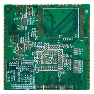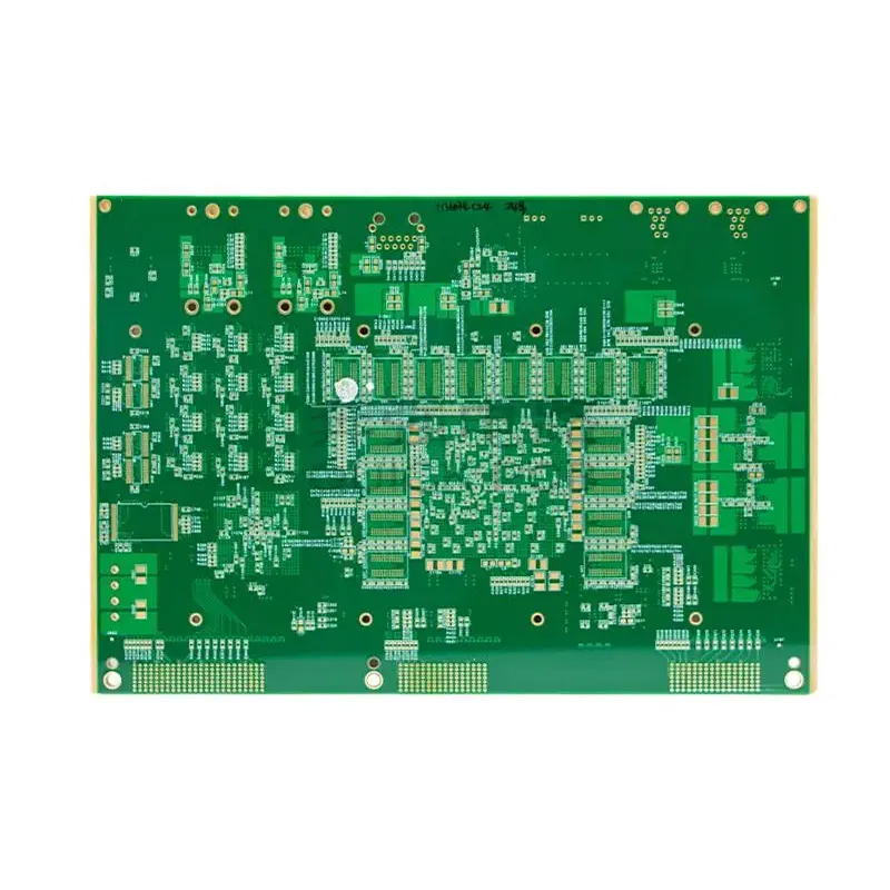
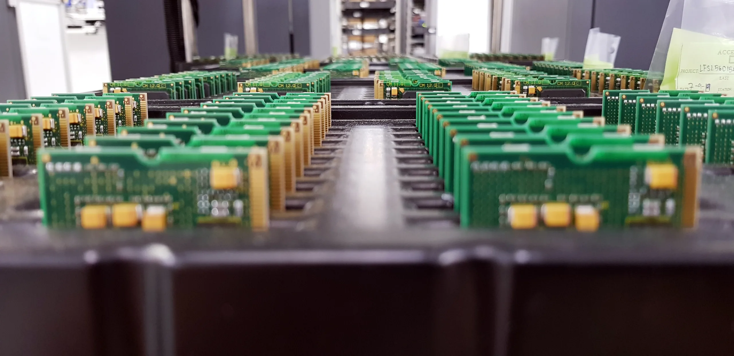

Product Overview: What Is a 10-Layer 3-Stage HDI PCB?
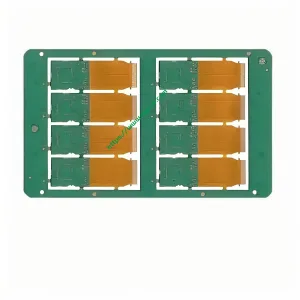
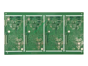
A 10-layer 3-stage HDI PCB is a high-density interconnect printed circuit board. It uses three sequential lamination cycles and three laser drilling steps. The 3+N+3 stackup has three build-up layers on each side. The middle N section contains four core layers. Total layer count is ten. This structure enables high-density routing and reliable signal transmission.

IPC-2226 defines this 3+N+3 structure as Type III HDI. Note: Some older sources call 3+N+3 Type II. That label is incorrect. IPC-2226 defines Type III for 3+N+3.
The electronics industry keeps shrinking devices. Traditional PCB technology is near its physical limits. HDI technology solves this problem. It packs more routing into less space. As a result, HDI PCBs power modern high-end electronics.
Core Specifications
| Parameter | Specification |
|---|---|
| Layer count / stage | 10 layers / 3-stage (3+N+3) |
| Base material | FR4 Tg170 (IPC-4101) |
| Board thickness | 1.2 mm |
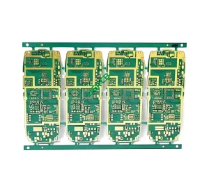
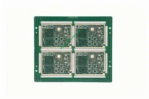
| Panel size | 126 × 118 mm / 4-up |
| Outer copper thickness | 35 μm (approx. 1 oz) |
| Inner copper thickness | 18 μm (approx. 0.5 oz) |
| Minimum through hole | 0.20 mm |
| Minimum blind via | 0.10 mm |
| Minimum BGA | 0.25 mm |
| Line width and spacing | 2.8/3.2 mil (0.071/0.081 mm) |
Industry Standard Classification: HDI Types Under IPC-2226
IPC-2226 defines HDI types by build-up layers per side.
| HDI Type | Stackup | Build-Up Layers Per Side | IPC-2226 Status |
|---|---|---|---|
| Type I | 1+N+1 | 1 | Standard type |
| Type II | 2+N+2 | 2 | Standard type |
| Type III | 3+N+3 | 3 | Standard type |
| ELIC | Any-layer | 3+ | Industry term, not an IPC-2226 type |
This product is IPC-2226 Type III. It uses 3+N+3. It supports 0.25 mm BGA pitch. It also supports 0.10 mm blind vias.

IPC-T-50M defines a microvia as a blind via with:
- Diameter ≤ 0.15 mm
- Aspect ratio ≤ 1:1
- Depth ≤ 0.25 mm
UGPCB’s 0.10 mm blind via meets this definition.
Stackup Structure: Engineering Logic of 3+N+3
The 3+N+3 stackup uses three build-up layers on each side. For a 10-layer board, N equals 4. The full stackup is 3+4+3.
- Outer layers: three signal layers on each side.
- Middle layers: four core layers.
- Inner layers: power and ground planes.

This arrangement supports high-speed signals and stable power delivery.
Key design points:
- Signal integrity: Control 50 Ω single-ended impedance. Control 90 Ω and 100 Ω differential impedance.
- Power distribution: Use split power and ground planes. Keep inner copper at 18 μm or higher.
- Microvia design: Follow IPC-2226. Keep microvia aspect ratio at or below 1:1.
- BGA fanout: Support 0.25 mm BGA pitch. This pitch suits advanced packages.
How It Works: Microvia Technology for High-Density Interconnect
HDI PCBs use microvias instead of through holes. A microvia connects only the layers that need a connection. This design frees routing space.
UGPCB builds this 10-layer 3-stage HDI PCB in three stages.
- Stage 1: Laser drills form blind vias between L1-L2 and L9-L10.
- Stage 2: Laser drills form blind vias between L2-L3 and L8-L9.
- Stage 3: Laser drills form blind vias between L3-L4 and L7-L8.
Three lamination cycles build all microvia layers. This process creates a true 3D interconnect structure.
Reliability matters. IPC-6012 Class 3 requires a minimum of 20 μm copper in holes. It also requires an average of 25 μm. Plating must reach the bottom of each blind via. Engineers control aspect ratio to prevent voids.
Key Materials and Performance
FR4 Tg170 Base Material
This product uses FR4 Tg170 laminate. It meets IPC-4101. Tg means glass transition temperature. Tg170 means the material stays rigid below 170°C.
High-Tg materials offer key benefits:
- Thermal reliability: Z-axis CTE is about 45–55 ppm/°C below Tg. IPC-4101 sets a maximum of 60 ppm/°C for many high-Tg FR4 grades.
- Solderability: The material withstands lead-free reflow. Peak temperature reaches about 260°C.
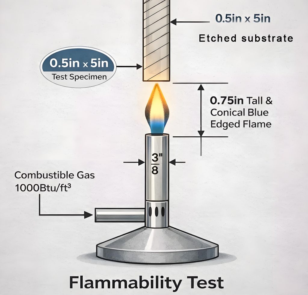
- Flame rating: FR4 meets UL94 V-0. It self-extinguishes within 10 seconds. It does not produce flaming drips that ignite cotton.
Copper Thickness
- Outer copper: 35 μm, about 1 oz. It carries current and spreads heat.
- Inner copper: 18 μm, about 0.5 oz. It supports fine-line etching.
Line Width and Spacing
The board achieves 2.8/3.2 mil line width and spacing. That equals 0.071/0.081 mm. This range falls into fine-line PCB design.
IPC-2221B requires 0.10 mm minimum spacing for external uncoated conductors at 0–15 V. This product’s 3.2 mil spacing is close to that limit. It demands tight etching control and high-precision AOI.
Manufacturing Process: From Core to Finished HDI PCB
UGPCB follows a multi-stage sequential lamination process.
Stage 1: Core Fabrication
The process starts with double-sided copper-clad laminate. Mechanical drilling forms through holes down to 0.20 mm. Plating, imaging, and etching form inner-layer circuits.
Stage 2: First Build-Up Lamination and Laser Drilling
The team stacks prepreg and copper foil on both sides. A high-temperature press bonds the layers. A UV laser drills 0.10 mm blind vias. Plating fills the vias and forms L1-L2 interconnects.
Stage 3: Second Build-Up Lamination and Laser Drilling
The team repeats lamination, laser drilling, and plating. This step forms L2-L3 interconnects.
Stage 4: Third Build-Up Lamination and Laser Drilling
The team completes the third build-up. This step forms L3-L4 interconnects. All ten layers now have interconnections.
Stage 5: Outer Patterning and Finishing
The process forms outer circuits with 2.8/3.2 mil line width and spacing. Then comes solder mask, surface finish, and routing. Surface finish options include ENIG, OSP, and lead-free HASL. Final checks include AOI, X-ray, and flying probe testing.
Applications of 10-Layer 3-Stage HDI PCB
5G Communication Equipment
5G smartphones need high routing density. The 10-layer 3-stage HDI PCB supports 0.25 mm BGA and mmWave modules. UGPCB’s HDI PCB solutions serve this market.
AI Servers and High-Performance Computing
AI servers use FPGAs and GPUs with high pin counts. A 10-layer 3-stage HDI PCB provides fine lines and small vias. It supports high-speed interconnects.
Automotive Electronics
Advanced driver-assistance systems use radar, LiDAR, and domain controllers. These systems need high-frequency HDI boards. The 10-layer 3-stage HDI PCB meets that need.
High-End Consumer Electronics
Flagship tablets, wearables, and imaging devices benefit from HDI technology. They gain thinner designs and better performance.
Why Choose UGPCB for Your 10-Layer 3-Stage HDI PCB?
UGPCB offers high-order HDI mass production. We build 1-stage to 3-stage HDI PCBs and beyond.
We follow IPC standards. Our process covers IPC-2226 design rules and IPC-6012 acceptance criteria.
We use high-quality FR4 Tg170 laminate. The material meets IPC-4101 and UL94 V-0.
We deliver fine-line capability. Our lines reach 2.8/3.2 mil. Our laser vias reach 0.10 mm.
We provide PCB and PCBA turnkey services. You can source bare boards and full PCBA assembly from one partner.
Get a Quote for Your HDI PCB Project
Need a 10-layer 3-stage HDI PCB quote? Need HDI PCB prototyping? Need PCBA turnkey service?
UGPCB offers:
- Free technical review and stackup advice
- Fast prototyping
- Flexible volumes from small batch to mass production
Contact UGPCB today. Upload your Gerber files and technical requirements. Our engineers will reply within 24 hours with pricing and technical feedback.
Visit UGPCB’s website to start your HDI PCB order.
Product parameters come from UGPCB’s manufacturing data. Industry process descriptions come from public technical references.
Data Source Declaration
This article cites the following standards and sources:
- IPC-2226, Design Guidelines for High Density Interconnect Structures. Defines HDI Type I, Type II, and Type III. Defines 3+N+3 as Type III.
- IPC-6012, Qualification and Performance Specification for Rigid Printed Boards. Class 3 requires 20 μm minimum and 25 μm average copper in holes.
- IPC-4101, Specification for Base Materials for Rigid and Multilayer Printed Boards. Covers FR4 Tg170 and Z-axis CTE limits.
- IPC-2221B, Generic Standard on Printed Board Design. Lists 0.10 mm minimum spacing for external uncoated conductors at 0–15 V.
- IPC-T-50M, Terms and Definitions for Interconnecting and Packaging Electronic Circuits. Defines microvia as ≤ 0.15 mm diameter, ≤ 1:1 aspect ratio, and ≤ 0.25 mm depth.
- UL 94, Tests for Flammability of Plastic Materials for Parts in Devices and Appliances. UL94 V-0 requires self-extinguishing within 10 seconds and no flaming drips that ignite cotton.
- UGPCB product specification sheet for the 10-layer 3-stage HDI PCB.