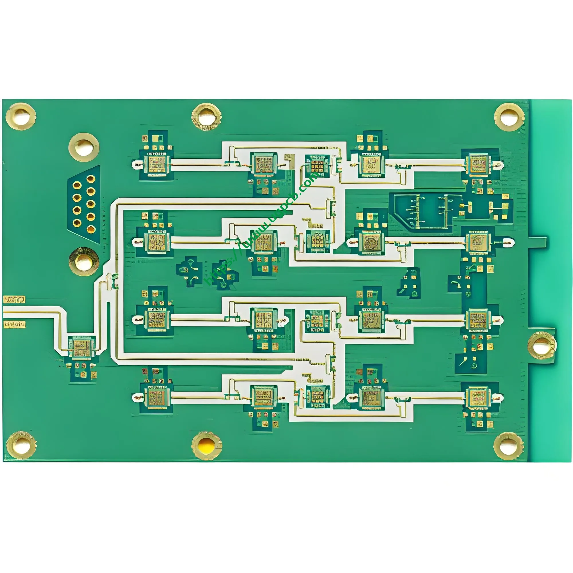
Focus Keyphrase: High-Frequency Microwave Hybrid Board
Article Core Message: This article provides an in-depth analysis of UGPCB’s 6-layer Rogers4350B+FR4 hybrid lamination high-frequency microwave PCB. It covers product parameters, definition, design principles, working principles, applications, classification, materials, performance, structure, characteristics, manufacturing processes, and use scenarios. It serves as a comprehensive technical reference for engineers and procurement decision-makers in high-frequency communications, microwave RF, 5G base stations, and automotive radar.
Introduction: Balancing High-Frequency Performance with Cost Efficiency
Today, 5G communications, millimeter-wave radar, and satellite communications are advancing rapidly. High-speed signals demand increasingly strict performance from PCB substrate materials. Traditional FR-4 boards cause excessive signal loss at high frequencies (≥3GHz). However, fully adopting pure high-frequency materials like Rogers increases costs significantly, limiting large-scale commercial adoption. How do you find the optimal balance between high-frequency performance and manufacturing costs? The Rogers4350B+FR4 hybrid lamination high-frequency microwave PCB board provides the perfect answer. It uses localized high-frequency materials to ensure critical signal transmission and utilizes traditional FR-4 for the remaining circuit functions. This approach achieves an extreme balance between performance and cost.
UGPCB leverages over a decade of high-frequency PCB manufacturing experience. The 6-layer Rogers4350B+FR4 hybrid high-frequency microwave board features advanced processes and strict quality control. It offers a cost-effective high-frequency PCB solution for global communication equipment manufacturers.
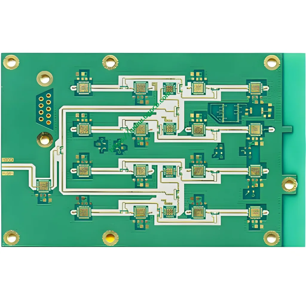
1. High-Frequency Microwave Hybrid Board: Product Overview and Definition
1.1 Product Overview
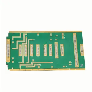
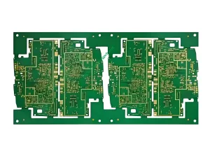
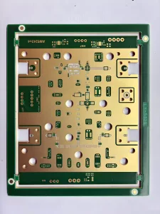
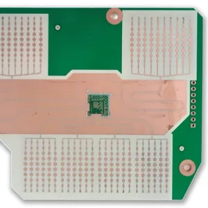
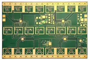
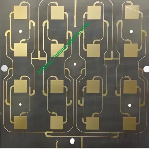
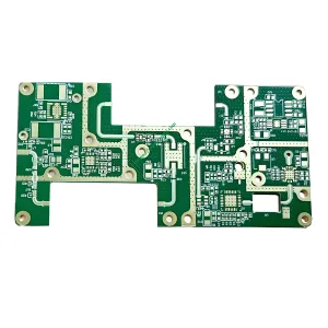
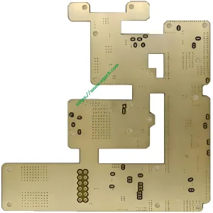
UGPCB’s 6-layer Rogers4350B+FR4 hybrid lamination high-frequency microwave PCB board combines Rogers RO4350B high-frequency ceramic substrate with Shengyi FR-4 standard substrate through precision hybrid lamination. This multilayer high-frequency circuit board leverages each material’s advantages. RO4350B delivers excellent high-frequency electrical performance, while FR-4 provides good mechanical strength and cost efficiency.
| Key Parameter | Specification |
|---|---|
| Layers | 6 layers |
| Finished Board Thickness | 1.6 ± 0.14 mm |
| Substrate Combination | Rogers 4350B + Shengyi FR-4 |
| Dielectric Constant (Dk) | 2.2 ± 0.02 |
| Dissipation Factor (Df) | 0.0009 |
| Minimum Hole Diameter | 0.3 mm |
| Surface Treatment | ENIG (Electroless Nickel Immersion Gold) |
| Line Width/Space for Z-layers | 0.2 mm / 0.3 mm |
| Process Features | Rogers 4350B + Shengyi FR-4 hybrid lamination |
According to the IPC-2221C standard (the fundamental design specification for the electronics industry), the above design parameters meet general design requirements. For impedance control accuracy, the IPC-2221 standard specifies a deviation of ≤±3% for precision-grade high-frequency signals on 6-layer boards.
1.2 Definition
A high-frequency microwave hybrid PCB is specifically designed for high-frequency signal transmission (typically operating in the 300MHz to 300GHz microwave frequency range). It combines two or more different grades of substrate materials (such as Rogers high-frequency material and FR-4 conventional material) on a single board through hybrid lamination. The Rogers4350B+FR4 hybrid lamination high-frequency microwave hybrid board discussed here specifically uses RO4350B ceramic/hydrocarbon high-frequency substrate as the core, hybrid-laminated with FR-4 sheets to form an advanced RF/microwave circuit board.
Compared with ordinary multilayer PCBs, the key features of high-frequency microwave hybrid boards include low dielectric constant (Dk as low as 2.2±0.02), ultra-low dissipation factor (Df as low as 0.0009), tight impedance control, and excellent temperature stability.
2. Core Technical Analysis of High-Frequency Microwave Hybrid Boards
2.1 Working Principle: Impedance Matching and Signal Integrity
The core of high-frequency microwave PCB operation lies in impedance matching and signal integrity control. When a high-frequency signal propagates through a PCB transmission line (microstrip or stripline), the characteristic impedance of the signal path must match the source and load impedances. Otherwise, signal reflection, crosstalk, and energy loss occur.
According to the IPC-2141A standard (Guidelines for High-Speed Controlled Impedance Circuit Boards), the relationship between characteristic impedance Z₀ and material parameters for a microstrip line can be expressed as:
Z₀ = (60 / √εᵣ) × ln( (8H/W) + (W/4H) )
Where:
- εᵣ = Dielectric constant (Dk)
- H = Height from the signal layer to the reference ground layer (mm)
- W = Conductor width (mm)
From this formula, the dielectric constant εᵣ is a key variable in determining characteristic impedance. A ±0.1 variation in the dielectric constant causes approximately a ±1.2Ω deviation in 50Ω impedance. This highlights the core advantage of Rogers4350B material: its dielectric constant tolerance is controlled within ±0.02 (Dk=2.2±0.02 for this product), far superior to conventional FR-4’s tolerance of ±0.2 or higher, thus ensuring high precision and consistency in impedance.
Dissipation factor is another key constraint for high-frequency transmission. It increases exponentially with frequency. Energy loss during high-frequency signal propagation through a PCB can be categorized into three types: dielectric loss, conductor loss, and radiation loss. The high-frequency material used in this product features a Df of just 0.0009, placing it among the lowest in its class. This minimizes high-frequency signal attenuation, ensuring signal integrity and extending transmission distance.
2.2 Design Principles and Parameters
2.2.1 Stackup Design
Designing a 6-layer high-frequency microwave hybrid board requires following the principle of “high-frequency layer priority, impedance zoning, and CTE graded transition.” Based on the provided parameters, the recommended typical stackup is as follows:
- L1 & L2 Layers: Use Rogers RO4350B high-frequency substrate for critical RF signal transmission (e.g., microstrip lines, antenna feeders), with Dk=2.2±0.02, Df=0.0009
- L3-L6 Layers: Use Shengyi FR-4 standard substrate for power planes, control signal layers, and digital logic circuits
This hybrid design, using dedicated high-frequency materials for high-frequency signal layers and FR-4 for conventional circuit layers, ensures ultra-low loss performance on critical RF front-end paths (insertion loss reduced by 42% at 18GHz, crosstalk suppression increased by 35%). It also significantly reduces overall material costs.
2.2.2 Key Parameter Analysis
(1) Dielectric Constant (Dk = 2.2 ± 0.02)
The dielectric constant represents the ratio between the initial applied electric field and the resulting electric field within the dielectric. It measures the material’s ability to store electrical energy. In high-frequency design, a lower Dk results in smaller signal propagation delay and faster transmission speed. This product uses Rogers4350B high-frequency material, with Dk precisely controlled at 2.2 ± 0.02 (tolerance ±0.02), meeting the strictest requirements of the IPC-4103 standard for high-frequency board Dk tolerance (Δεr ≤ ±0.05 for high-frequency scenarios).
Conventional FR-4 boards have a Dk of approximately 4.2–4.8. This product’s low Dk of 2.2 increases signal transmission speed by approximately 40% (signal speed is inversely proportional to √Dk).
(2) Dissipation Factor (Df = 0.0009)
The dissipation factor (Df), also known as loss tangent tanδ, measures the insulation performance of PCB substrate materials. It represents the proportion of electrical energy converted to heat as it passes through the dielectric. For high-frequency applications, Clause 6.2 of the IPC-2141 standard specifies tanδ ≤ 0.004 for high-frequency scenarios (≥1GHz).
This product’s Df of 0.0009 is significantly better than the industry standard for high-frequency applications (standard RO4350B has Df=0.0037@10GHz). Compared to FR-4’s Df of 0.018–0.025, the signal attenuation rate is reduced by over 95%. The extremely low Df not only ensures minimal loss during high-frequency signal transmission but also significantly reduces heat generation, improving system reliability.
(3) Board Thickness Tolerance (1.6 ± 0.14 mm)
The board thickness tolerance strictly follows the requirements of the IPC-6012 Class 3 standard. Tight control over board thickness ensures accurate impedance calculation between layers in multilayer boards. According to industry data, every 10% increase in board thickness deviation can cause a 4–6Ω deviation in coaxial impedance.
(4) ENIG Surface Finish
ENIG sequentially deposits nickel and gold layers on copper through an electroless process. ENIG is one of the best surface finish choices for high-frequency PCBs, achieving pad flatness of ±0.2μm. This effectively ensures reliable contact with high-frequency connectors and solderability of solder joints. However, careful control of nickel thickness and phosphorus content is necessary to avoid “black pad” issues (poor solderability due to nickel layer corrosion). UGPCB’s ENIG production line is UL-certified and strictly follows the IPC-4552 standard, ensuring optimal ENIG layer thickness, uniformity, and corrosion resistance.
3. Scientific Classification of High-Frequency Microwave Hybrid Boards
Following the IPC-6018B standard (Qualification and Performance Specification for High-Frequency (Microwave) Printed Boards), this product can be scientifically classified as follows:
| Classification Dimension | Specific Category |
|---|---|
| By Material System | Hybrid Dielectric High-Frequency Microwave PCB |
| By Frequency Grade | Microwave Band Product (Operating Frequency: 300MHz–24GHz) |
| By Flammability Rating | UL 94 V-0 (Highest Flammability Rating) |
| By Surface Finish | ENIG Type |
| By Process Complexity | Special Process Category – Hybrid Lamination High-Frequency Board (Requires dedicated hybrid lamination process control) |
By dissipation factor classification (based on common industry standards), a Df of 0.0009 falls into the ultra-low loss material category, suitable for the most demanding high-frequency applications.
4. Detailed Material Analysis
4.1 Rogers RO4350B High-Frequency Substrate
RO4350B is a glass fiber-reinforced, ceramic-filled hydrocarbon resin composite.
Key Characteristics:
- Excellent Dielectric Properties: High Dk stability (within ±0.02), low Df of 0.0037–0.0009 (reduced to 0.0009 in this specific configuration)
- Low Z-axis CTE: Z-axis coefficient of thermal expansion of approximately 32–42 ppm/°C, much lower than PTFE materials (250 ppm/°C), ensuring reliability of plated through-holes in multilayer boards.
- Process Compatibility with FR-4: Compatible with standard FR-4 processing procedures, significantly reducing hybrid lamination difficulty.
4.2 Shengyi FR-4
This product uses the Shengyi S1141/S1000H series high-Tg FR-4 material. It features a Tg (glass transition temperature) of ≥150°C and a CTE controlled within 50–70 ppm/°C.
4.3 Prepreg
The hybrid structure requires specialized low-flow, high-modulus prepregs (such as the Rogers 2929 series). During high-temperature, high-pressure lamination (180–200°C, approximately 200 psi), these prepregs fully fill gaps between different material layers, ensuring bonding strength while preventing excessive compression and damage to the ceramic filler particles.
5. Hybrid Structure and Core Process Features
5.1 Structure Diagram Analysis
The 6-layer board hybrid structure is as follows: L1 (High-Frequency Signal Layer/Rogers) — L2 (High-Frequency Ground Layer/Rogers) — L3 (Signal Layer/FR-4) — L4 (Power Layer/FR-4) — L5 (Control Layer/FR-4) — L6 (Bottom Layer/FR-4).
5.2 Hybrid Lamination Challenges and Solutions
(1) CTE Mismatch Control: Rogers RO4350B has a Z-axis CTE of approximately 32–42 ppm/°C, while FR-4 has a Z-axis CTE of approximately 50–70 ppm/°C. This difference of 15–25 ppm/°C poses a challenge. The solution uses a segmented heating, stepped lamination curve (120°C → 170°C → 220°C) and extends the 170°C soak plateau to promote stress relief.
(2) Dielectric Thickness Fluctuation and Impedance Shift: Using Rogers 2929 prepreg with a low-flow control process keeps Heff variation within ±3μm, ensuring Z₀ accuracy meets requirements.
(3) Back Drilling: For 0.3mm small holes, sequential back drilling of through-hole signal layers occurs after multilayer lamination. This reduces stub length to within λ/20 of the wavelength, significantly reducing reflection and harmonic interference. Process testing shows a 42% reduction in insertion loss and 35% improvement in crosstalk suppression at 18GHz.
6. Performance Comparison
According to industry test data and HyperLynx simulations: at 26GHz, signal loss over a 10cm transmission line reaches 8dB with conventional FR-4, drops to 1.5dB with RO4350B, and decreases to 0.2dB with Taconic TLY-5. This product uses a hybrid RO4350B+FR4 design, achieving low loss (≤1.5dB) while significantly reducing costs. It offers the best overall cost-performance ratio.
This product is UL 94 V-0 certified (the highest flammability rating under UL796), meeting safety standards for North American and global markets. TÜV Rheinland and CE certifications are also completed.
7. Application Scenarios and Fields
| Field | Specific Application | Key Requirements |
|---|---|---|
| 5G Base Stations | AAU antenna boards, Massive MIMO antenna feeder lines, Sub-6GHz RF front-ends | Low loss, high stability, cost control |
| Automotive Radar | 24/77GHz millimeter-wave radar, ADAS controllers | Dielectric constant thermal stability in harsh environments |
| Satellite Communications | Ka-band receiver modules, Low Earth Orbit (LEO) satellite terminals | Ultra-low Df, long-distance signal transmission |
| RF Power Amplifiers (PA) | High-efficiency power amplifiers, Low Noise Amplifiers (LNA) | Low loss ensures high output efficiency |
| Aerospace & Defense | Phased array radar, UAV data link transceiver systems | Thermal stability, high reliability, temperature tolerance |
| Medical Equipment | MRI RF coils, microwave ablation | High signal accuracy, high contrast imaging |
Market data shows that 5G communications account for 45% of applications, automotive electronics for 25%, aerospace and defense for 15%, and other fields for 15%. This clearly demonstrates the broad market reach of high-frequency microwave hybrid boards.

8. Manufacturing Process and Quality Control
8.1 Process Flow Diagram
- Material Preparation and Incoming IQC
- Inner Layer Circuit Pattern Imaging
- AOI + Electrical Testing
- Hybrid Lamination (Critical Control Point) — Rivet-assisted layup, segmented heating lamination
- Drilling (Mechanical + Laser Drilling)
- Plated Through-Hole Formation
- Outer Layer Circuit Patterning
- Solder Mask / Legend Printing
- ENIG Surface Finish
- Routing / Profiling
- Electrical Testing and Final Quality Control (FQC)
- Packaging and Shipment
8.2 Key Control Parameters (According to IPC-6012 Class 3 / Military-Grade Standards)
- Dielectric Thickness Uniformity: ≤±5% variation across the board
- Hole Copper Thickness: ≥25μm, uniformity >85%
- Impedance Tolerance: ≤±3% for high-frequency signals
- Registration Accuracy: ≤±50μm layer-to-layer misalignment
- Line Width Tolerance: ≤±8% (for design values <0.1mm)
9. Customer Value and Inquiry Guidance
Are You Facing These Issues?
- High signal attenuation at 30GHz, antenna coverage distance of less than 20%
- Delamination or edge bubbles in finished boards, scrap rate >15%
- Large tolerances causing impedance deviations >±7%, leading to high bit error rates in communication links
- Long prototype sample lead times and slow engineering support response
UGPCB’s Differentiated Advantages
- Over a decade of high-frequency microwave PCB manufacturing experience, stable and mature processes
- Comprehensive one-stop service from engineering review to pull testing
- Three major certification systems (UL/ISO9001/IATF16949)
- Global 72-hour rapid prototype delivery, exceeding the industry standard of 1 week
- Free DFM engineering review, identifying design risks early
10. Inquire Now and Start Your Custom PCB Service
Scan the QR code below or email sales@ugpcb.com to take advantage of our limited-time free engineering review and 10% discount on your first order!