
In today’s rapid evolution toward lightweight, thin, short, and compact electronic devices, the rigid-flex PCB has become indispensable in high-precision fields such as telecommunications, medical instruments, and aerospace. Its unique combination of rigid support and three-dimensional flexibility makes it a critical interconnect component.
As a professional PCB manufacturer, UGPCB introduces its high-performance Yellow Soldermask Rigid-Flex PCB (R-FPCB) . This article explores this advanced board, built with FR-4 + PI materials and a 6-layer rigid plus 4-layer flexible structure. We will examine its design principles, manufacturing processes, and applications, showing how it enables more stable signal transmission and a more compact system layout.
1. Product Definition and Overview
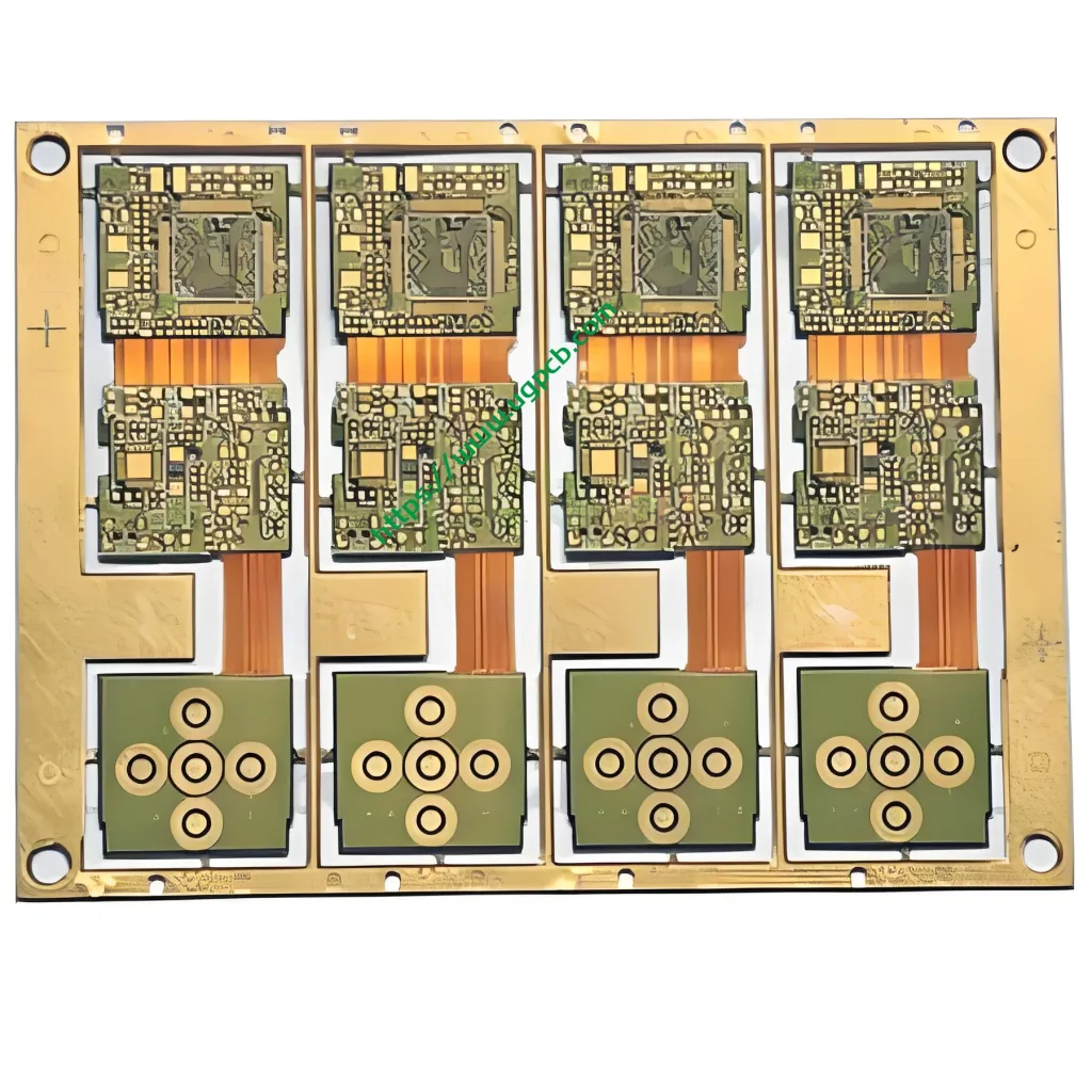
UGPCB’s Yellow Soldermask Rigid-Flex Board integrates a rigid PCB and a flexible circuit board into a single interconnect solution through a lamination process.
Key Specifications:
Layer Stackup: 6 layers (6L) in rigid sections / 4 layers (4L) in flexible sections
Material Combination: FR-4 (rigid areas) + PI (Polyimide, flexible areas)
Surface Color: Yellow soldermask (rigid) / White coverlay (flex)
Finished Thickness: 0.4mm (rigid sections) / 0.2mm (flex sections)
This design retains the structural support and component-carrying capacity of rigid areas while utilizing the bendability of flexible sections. It achieves a true rigid-flex integration, eliminating the need for traditional connectors and ribbon cables.
2. Design Principles and Technology
A. Working Principle
The core of rigid-flex technology lies in seamless interconnection. UGPCB laminates flexible PI layers with rigid FR-4 layers under high temperature and pressure. In flexible zones, FR-4 material is removed, leaving the PI base with a coverlay to allow bending. In rigid zones, FR-4 remains to support components. This structure eliminates physical contact points from connectors, significantly enhancing signal integrity (SI) and vibration resistance.
B. Design Considerations
Impedance Control: For high-frequency communication PCBs, strict control of 3.5mil trace width and spacing ensures consistent differential impedance (e.g., 100Ω).
Transition Zone Protection: The junction between rigid and flexible sections (the stub) is a stress point. UGPCB’s design uses rounded transitions and tapered trace widths to prevent cracking during bending.
Stackup Matching: Uniform 1OZ copper thickness is maintained to prevent fatigue failure in the flexible sections during dynamic flexing.
3. Material and Performance Analysis
A. Core Materials
FR-4 (Rigid Areas): A fiberglass-reinforced epoxy laminate. It offers high mechanical strength, heat resistance, and insulation, providing a stable platform for mounting heavy components like chips and connectors.
PI (Flexible Areas): Polyimide film. It provides excellent high-temperature resistance (operating >150°C), a low dielectric loss factor (Df), and a high flex life.
Surface Finish: Immersion Gold (ENIG). This chemical process deposits a nickel-gold layer over copper.
Advantages: High surface flatness suitable for fine-pitch circuits (3.5mil spacing), strong oxidation resistance, and good solderability along with aluminum wire bonding capability.
B. Key Performance Specifications
| Parameter | Specification | Technical Advantage |
|---|---|---|
| Min. Trace/Space | 3.5mil / 3.5mil | Supports high-density routing for compact communication modules. |
| Min. Mechanical Drill | 0.1mm | Micro-via technology improves routing channel utilization and reduces interlayer parasitic capacitance. |
| Finished Thickness | 0.4mm (Rigid) / 0.2mm (Flex) | Ultra-thin design saves space inside the device enclosure. |
| Copper Thickness | 1OZ (35μm) | Balances current-carrying capacity with flexural endurance, ensuring signal integrity. |
4. Structural Classification and Features
A. Structural Classification
This product is an asymmetric structure (6-layer rigid + 4-layer flexible) within the category of multi-layer rigid-flex boards. Generally, rigid-flex boards are classified as:
Layered Type: Flexible layers extend out independently, as seen in this product.
Non-layered Type: The entire board uses flexible material, with stiffeners added to specific areas.
B. Product Features
High Reliability: The immersion gold finish combined with PI material ensures stable electrical performance even in harsh environments (high temperature and humidity).
High Precision: Manufacturing capabilities for 3.5mil fine lines and 0.1mm micro vias solve high-density interconnect challenges.
Space Optimization: Replaces connectors, reducing installation volume by over 60% and lowering overall product weight.
Visual Differentiation: The yellow soldermask provides a unique appearance and offers clearer contrast during SMT assembly, facilitating optical inspection.
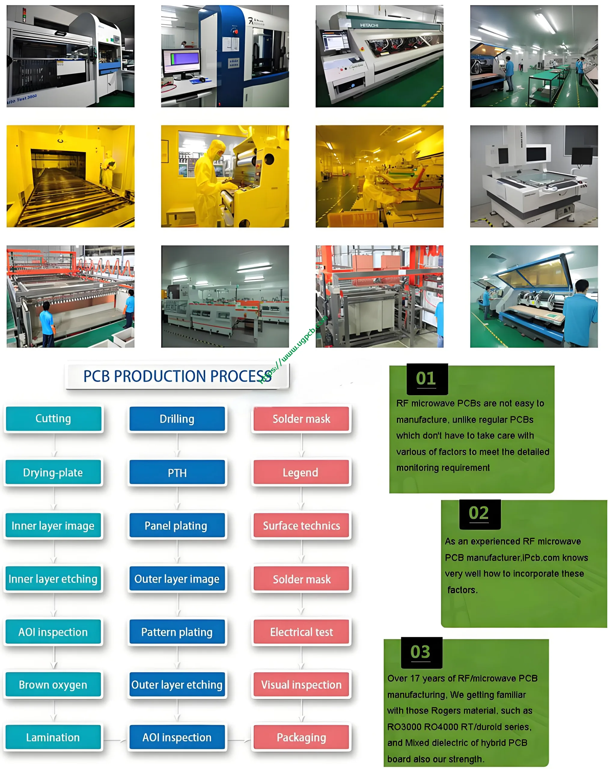
5. Manufacturing Process and Quality Control
To ensure the reliability of this complex 6L+4L structure, UGPCB follows a rigorous production flow:
Inner Layer Circuit (Flex Area): Fine 3.5mil circuits are formed on the PI base material using laser or photolithography.
Coverlay Lamination: A protective film is laminated onto the flexible circuit, leaving only the pad areas exposed.
Lamination: Rigid and flexible layers are aligned and laminated under vacuum. Key controls are the temperature profile and resin flow to prevent voids.
Drilling & Plating: 0.1mm micro vias are drilled. Electroless copper deposition creates interlayer connections.
Outer Layer & Soldermask: Yellow soldermask is applied to rigid areas; white coverlay remains on flexible areas.
Surface Finish: Immersion gold (ENIG) is applied with controlled thickness: 0.05-0.1μm Au / 3-5μm Ni.
Profiling & Electrical Test: Laser routing or die punching defines the final shape. 100% AOI and flying probe testing verify electrical integrity.
6. Applications
This product is primarily targeted at the communication PCB sector. Key applications include:
5G Communication Base Stations: Used for flexing connections in RF modules, solving compact interconnect needs between antennas and mainboards.
Smartphones & Wearables: The 0.2mm flexible section enables dynamic bending in foldable phone hinges.
Medical Electronics: Used in devices like ultrasonic endoscope probes, leveraging PI’s biocompatibility and high-density routing.
Automotive Electronics: ADAS camera modules that must withstand constant vibration and thermal shock.
7. Why Choose UGPCB?
Engineers often face challenges with low yields and long lead times for complex rigid-flex designs. UGPCB is a reliable supply chain partner offering:
Manufacturing Capability: Mass production capability for 3.5mil trace/space, overcoming high-density interconnect barriers.
Material Sourcing: Uses high-quality materials from suppliers like Shengyi/ITEQ for FR-4 and DuPont/Tayoho for PI, ensuring quality from the source.
Engineering Support: Provides free DFM (Design for Manufacturability) checks to help optimize designs, especially in the rigid-flex transition zone.
Are you designing a circuit board that must both carry complex ICs and flex within a tight space?
UGPCB now offers prototyping and mass production services for this 6-layer rigid + 4-layer flexible yellow soldermask rigid-flex PCB.
👉 Get a Quick Quote Today
Send your Gerber files and technical requirements to [sales@ugpcb.com] or click the online chat. Our engineering team will provide a professional DFM report and a competitive quote within 24 hours.


