
Capacidade de prototipagem de PCB da UGPCB: A Inovação Tecnológica & Referência do setor por trás da entrega rápida em 72 horas
PCB (Placa de circuito impresso) serve como o “esqueleto” e “sistema nervoso” da eletrônica moderna, agindo como o transportador principal conectando todos os componentes eletrônicos. De smartphones a comunicações via satélite, dispositivos médicos para sistemas de condução autônoma, sobre 99% dos dispositivos eletrônicos dependem da operação estável de PCBs de alto desempenho. Na competição acirrada do desenvolvimento de produtos, rápido, confiável, e de alta qualidade Serviços de prototipagem de PCB tornaram-se um fator decisivo para as empresas que desejam aproveitar as oportunidades de mercado. Aproveitando profundo conhecimento técnico e um sistema de fabricação avançado, UGPCB está redefinindo os padrões da indústria para giro rápido Fabricação de PCB.
🔍 eu. Prototipagem de PCB: A pedra angular e o teste decisivo da inovação eletrônica
A evolução dos PCBs abrange 130 anos. Desde a fiação manual antiga até a atual Interconexão de alta densidade (IDH) e Substratos IC, seu desenvolvimento progrediu em sincronia com as revoluções da tecnologia eletrônica. A aplicação prática de Laminado revestido de cobre (Ccl) a tecnologia durante a Segunda Guerra Mundial foi um ponto de viragem crucial, substituindo a solda manual complexa e propensa a erros e estabelecendo as bases para a confiabilidade, estabilidade, e miniaturização da eletrônica moderna.
-
Desafio do Engenheiro: Entregar um projeto de PCB com falhas não resolvidas à produção em massa leva a consequências catastróficas – falhas de desempenho, recalls caros, atrasos no projeto, perda de cliente, e danos à reputação da marca.
-
Solução UGPCB: Fornecendo abrangente, alta precisão, e resposta rápida Projeto de PCB e Serviços de prototipagem de PCB é a primeira e mais crítica salvaguarda para engenheiros que transformam conceitos inovadores em produtos confiáveis.
-
💡 Visão Profissional: O valor central de Prototipagem de PCB reside em “detecção precoce, correção precoce.” As estatísticas mostram que corrigir erros durante a fase de protótipo custa apenas 1/100 (ou menos) dos custos incorridos durante a produção em massa. UGPCB's prototipagem rápida de PCB capacidade é a chave para economizar significativamente os clientes R&D custos e tempo.
🛠️II. Mergulho profundo: Principais capacidades técnicas da UGPCB em prototipagem de PCB
As capacidades de fabricação da UGPCB cobrem tudo, desde placas simples/dupla face até placas de última geração Substratos de embalagem IC, apresentando parâmetros rigorosos e processos líderes do setor.
📊 1. Parâmetros principais do processo & Especificações Técnicas (Visão geral dos recursos de prototipagem de PCB UGPCB)
-
Dados principais:
-
Faixa de espessura da placa: Individual/Duplo: 0.10milímetros – 8.0milímetros (4 mil – 315 mil); Multicamadas: 0.15milímetros – 8.0milímetros (6 mil – 315 mil)
-
Min. Tamanho finalizado: 0.5 x 1,0 mm (Capacidade extrema de miniaturização)
-
Máx.. Camadas: Padrão: Até 100 camadas (Requer revisão); RF híbrida: 4-32 camadas
-
Alta Frequência/Especial Materiais: Rogers®, Arlon®, Taconic®, Isola® (FR408, 370RH), Teflon®/PTFE, Cerâmica, Cerâmica de Hidrocarbonetos, Materiais Híbridos
-
📡 2. Alta frequência & Prototipagem de PCB de alta velocidade: Chave para dominar a era do GHz
Impulsionado pelo aumento do 5G/6G, radar, comunicação por satélite (frequências >1GHz), e demandas de computação de IA, PCBs de alta frequência e alta velocidade são o ponto alto tecnológico. O principal desafio reside em controlar a perda de sinal e manter a estabilidade da impedância.
-
Desafios técnicos: Estabilidade da constante dielétrica (Dk) & Perda tangente (Df), rugosidade da superfície da folha de cobre, controle preciso da espessura da camada dielétrica.
-
Vantagens da UGPCB:
-
Experiência em Materiais: Processamento comprovado de topo laminados de alta frequência como Rogers® (RO3000™, Série RO4000®), Arlon® (Série AD/CL), Taconic® (RF-35, Série TLY), Isola® (FR408HR, Astra®).
-
Controle de impedância: Controle de tolerância rigoroso dentro de ±5%, frequentemente ±3%, atendendo aos mais exigentes integridade do sinal requisitos.
-
Aplicações: Mrink atrevido, cargas úteis de comunicação por satélite, equipamentos de rede de alta velocidade (400G/800G), instrumentos de teste de última geração.
-
-
📐 Fórmula Técnica – Impedância Característica (Modelo simplificado de microfita):
Z₀ ≈ (87 / √(εr + 1.41)) * ln(5.98h / (0.8w + t))-
Z₀: Impedância Alvo (Oh) -
εr: Constante dielétrica relativa do material do substrato -
h: Espessura dielétrica (mil) -
w: Largura do traço (mil) -
t: Espessura do traço (mil) -
Os engenheiros da UGPCB utilizam cálculos e simulações precisos para garantir impedância do circuito de alta frequência corresponde com precisão aos valores do projeto.
-
🔄 3. Prototipagem de PCB Rigid-Flex: O facilitador perfeito para projetos 3D complexos
PCBs rígidos e flexíveis combine o suporte estável de placas rígidas com a capacidade de flexão dinâmica de circuitos flexíveis, oferecendo uma solução revolucionária para miniaturização de dispositivos, redução de peso, e maior confiabilidade.
-
Vantagens únicas:
-
Reduz significativamente conectores e cabos, melhorando a confiabilidade do sistema (menos pontos de falha).
-
Adapta-se livremente a espaços 3D complexos, otimizando o layout interno do dispositivo.
-
Reduz o peso e o volume geral, ideal para dispositivos vestíveis, aeroespacial, e instrumentos médicos de precisão.
-
-
Desafios & Avanços na UGPCB:
-
Pontos de dor tradicionais: Processos complexos (até 50+ passos), altos custos de materiais, dificuldades de controle de rendimento, longos ciclos de produção.
-
Solução UGPCB: Otimizando a seleção de materiais (por exemplo, Correspondência de cobertura/adesivo PI), empregando laminação de alta precisão e perfuração a laser, implementando controle de processo rigoroso (por IPC-2223B, 6013Padrões D), aumentando efetivamente o rendimento e o encurtamento prazos de entrega do protótipo.
-
🧩 4. PCBs com alta contagem de camadas & Prototipagem de substrato IC: Habilitando Integração de Alta Densidade
Eletrônicos cada vez mais poderosos levam os PCBs a contagem de camadas altas (>10 camadas), roteamento de ultra-alta densidade, e embalagens avançadas. Substratos IC, agindo como o “intérprete” entre chips e placas-mãe, apresentam barreiras técnicas extremamente elevadas.
-
Tendências multicamadas: Diminuindo continuamente a largura/espaço da linha (L/S até ≤50μm/50μm), maior precisão para microvias (<100μm), alinhamento mais rigoroso camada a camada.
-
Substrato CI – O Núcleo da Embalagem:
-
Definição: PCBs de última geração montando diretamente o chip (Morrer), fornecendo interconexão elétrica, Gerenciamento térmico, e proteção física.
-
Principais características: Roteamento de ultra-alta densidade (Tecnologia HDI/SLP), núcleos ultrafinos (<100μm possível), linhas finas (L/S até 20μm/20μm), alta planicidade superficial, excelente gerenciamento térmico.
-
Força UGPCB: Possui maduro BGA (Array da grade de bola) e eMMC (MultiMediaCard incorporado) substrato capacidades de prototipagem e produção de volume baixo a médio, apoiando o cliente R&D em processadores, memória, Chips aceleradores de IA, e mais.
-
⏱️III. Velocidade & Vantagem de custo: Competitividade Central da UGPCB em Prototipagem de PCB
No mercado de eletrônicos onde “velocidade é fundamental,” a velocidade de prototipagem impacta diretamente Tempo até o mercado (TTM). Simultaneamente, o controle eficaz de custos é crucial para R&Orçamentos D.
-
Entrega rápida: UGPCB otimiza o fluxo de produção e o gerenciamento da cadeia de suprimentos. Prazos de entrega de protótipo de PCB padrão pode ser comprimido para um impressionante 72 horas (3 dias). Placas complexas (por exemplo, RF, IDH, rígido-flexível, >20 camadas) normalmente completa dentro 1-2 semanas (dependendo da complexidade), excedendo em muito as médias da indústria.
-
Estratégia de prototipagem de baixo custo:
-
Validação de Design Eficiente: Utiliza materiais econômicos comprovados e processos padronizados para rápida verificação funcional.
-
Soluções Flexíveis: Recomenda as combinações de materiais e processos mais econômicas com base nas necessidades de testes (desempenho elétrico, ajuste mecânico, função básica).
-
Proposta de valor: A validação antecipada do protótipo pode evitar até 90% de perdas potenciais durante a produção em massa. UGPCB's prototipagem de PCB de baixo custo é a escolha inteligente para gerenciar R&Risco D.
-
📌 Chamada para ação: Buscando Serviços de prototipagem de PCB que combinam velocidade, confiabilidade, e vantagem de custo? Contate UGPCB AGORA para um orçamento personalizado! Nós oferecemos DFM grátis (Design para fabricação) análise para otimizar seu design e acelerar o lançamento de produtos! [Clique na ferramenta de chat ao vivo no canto inferior direito para obter suporte técnico gratuito]
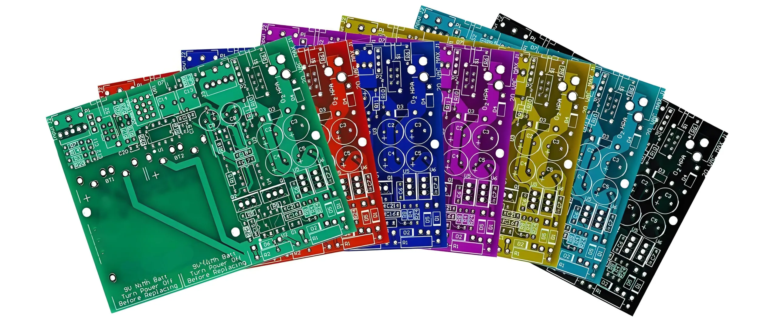
🎨IV. Além do Verde: A ciência e a arte da seleção de cores de PCB
Enquanto “engenharia verde” é o visual clássico do PCB, cores da máscara de solda oferecem muito mais variedade. UGPCB oferece opções como azul, amarelo, vermelho, preto, e branco – movidos não apenas pela estética, mas também funcionalidade:
-
PCBs brancos: Alta refletividade, aumenta significativamente a eficiência e a uniformidade da luz em Aplicações de iluminação LED.
-
PCB preto: Baixa refletividade, reduz a interferência de luz difusa, ideal para equipamentos de palco, produtos AV de última geração, transmitindo uma sensação profissional discreta.
-
Inspeção & Retrabalhar: Alto contraste entre fundos claros (amarelo, branco) e traços escuros (verde, azul) facilita a inspeção visual e o reparo manual.
-
Identidade da marca: Cores personalizadas fortalecem a identidade visual do produto e imagem da marca.
🚀V. Do design à produção em massa: Ciclo de valor da solução de PCB ponta a ponta da UGPCB
O valor da UGPCB vai muito além da fabricação de placas nuas, abrangendo todo o ciclo de vida do produto:
-
Suporte de projeto & Validação de protótipo (Valor Central): Prototipagem rápida fornece a janela dourada para encontrar e corrigir falhas de design, garantindo uma base robusta.
-
Função & Teste de desempenho: Engenheiros usam protótipos para integridade do sinal (E), integridade de energia (PI), simulação térmica, testes de estresse ambiental, etc., verificando o desempenho do produto sob várias condições.
-
Marketing & Potência de demonstração: Totalmente funcional PCBA protótipos são ideais para exposições, demonstrações de clientes, e propostas de financiamento, mostrando de forma tangível o valor do produto.
-
Rampa contínua para produção: Os processos de prototipagem da UGPCB se alinham estreitamente com as linhas de produção em massa, garantindo desempenho consistente e mitigando riscos de transição.
-
PCBA (Conjunto) Serviços de prototipagem: Ofertas completas Prototipagem PCBA incluindo fornecimento de componentes (Bom), Montagem SMT, THT (MERGULHAR) conjunto, e testes. A entrega de módulos funcionais prontos para execução acelera drasticamente o desenvolvimento do produto final e reduz o tempo de lançamento no mercado.
💎 Conclusão: Escolha UGPCB, Escolha um acelerador de inovação
Na indústria eletrônica em ritmo acelerado, tempo é participação de mercado, e a qualidade é fundamental. UGPCB, com seu:
-
Capacidades de processo de ponta (cobrindo RF/alta velocidade, rígido-flexível, contagem de camadas altas, Substratos IC),
-
Velocidade extrema de entrega (mais rápido 72 horas),
-
Estratégias de custos flexíveis (opções de validação de baixo custo),
-
Sistemas de qualidade rigorosos (cumprindo IPC, etc.),
-
Cadeia de serviços abrangente (suporte de projeto, Prototipagem de PCB, Montagem PCBA),
tornou-se o confiável Protótipo de PCB e parceiro de fabricação em volume para engenheiros globais e R&Equipes D. Seja em eletrônicos de consumo, eletrônica automotiva, dispositivos médicos, controle industrial, aeroespacial, ou comunicações, UGPCB fornece um sólido, rápido, e base física de alta qualidade para sua inovação.
Agir agora!
-
Obtenha sua cotação de protótipo de PCB personalizado
-
Consulte um especialista: Nossa equipe técnica está pronta para esclarecer suas dúvidas sobre projeto de alta frequência, estruturas rígidas-flexíveis, controle de impedância, Seleção de material, e mais.
-
Explore mais recursos:
Escolha UGPCB – Deixe-nos ser seu parceiro poderoso no caminho para o sucesso!
WeChat
Digitalize o código QR com WeChat