SMT Printing Yield Soars 60%! The Science Behind High-Precision PCB Stencil Design & Selection
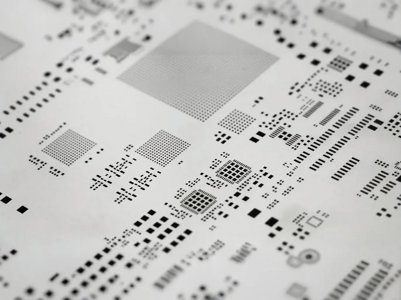
This ultra-thin stainless steel sheet carries the lifeline of modern electronics manufacturing – its microscopic apertures dictate the fate of billions of solder joints.
On SMT assembly lines, solder paste printing contributes to over 60% of process defects. Behind this staggering statistic often lies an underestimated critical tool: the PCB stencil.
The Critical Role of Stencils in SMT Processes
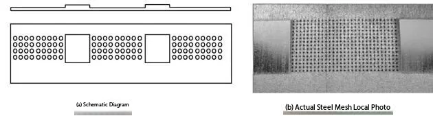
The stencil is the precision mold of modern electronics manufacturing. Its core function is depositing exact doses of solder paste onto designated PCB almofadas. This sheet, merely 0.08-0.18mm thick, directly determines solder joint quality and reliability.
As component miniaturization accelerates, 0201 componentes (0.6×0.3mm) and 0.35mm pitch BGAs have become mainstream. This poses severe challenges for stencil technology: when aperture sizes shrink below 150μm, paste release rates plummet to less than 70%.
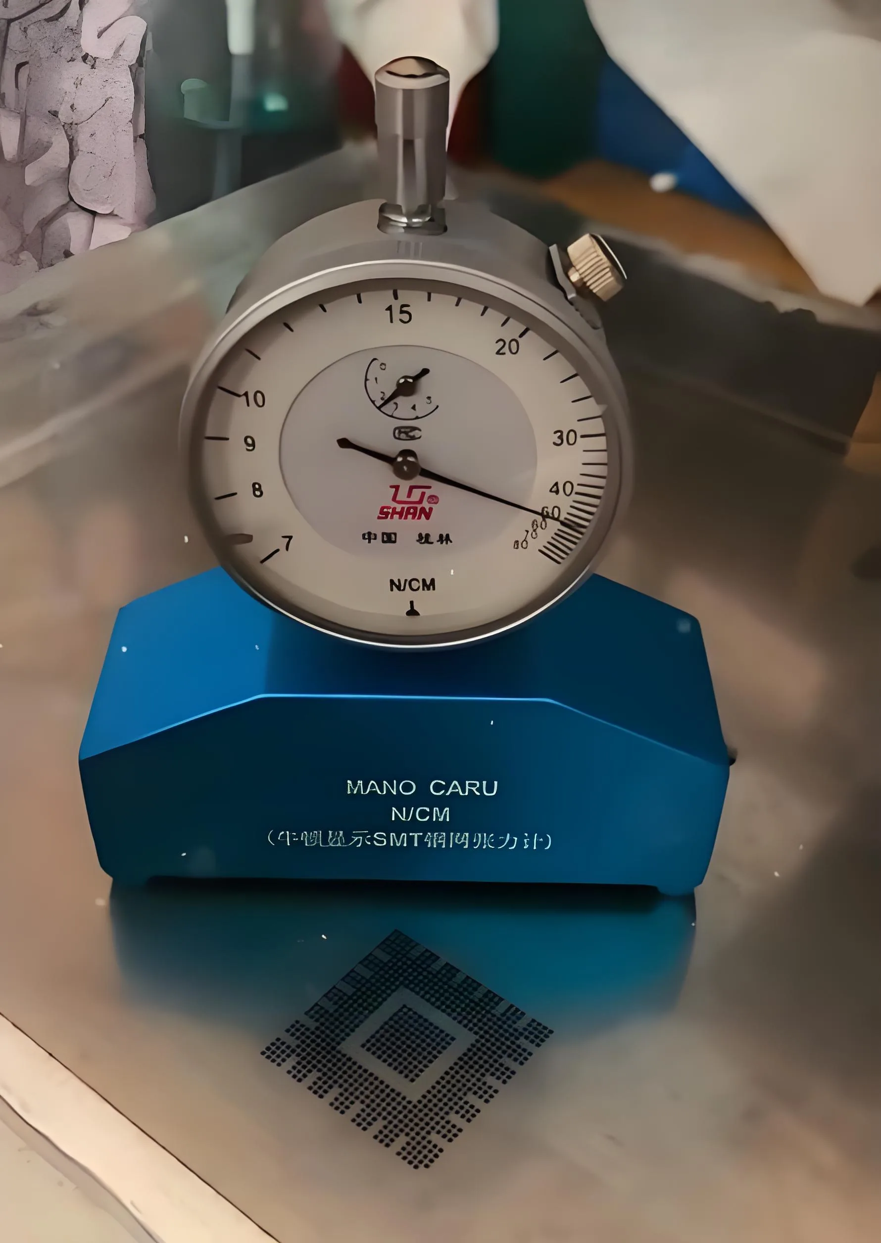
High-precision stencils must meet three core metrics simultaneously: tension stability at 35-50N/cm², surface flatness error <0.1mm/m², and aperture positional tolerance within ±15μm (for fine-pitch components below 0.4mm). These parameters directly impact printing accuracy and consistency.
Key Elements of Precision PCB Stencil Design
Scientific Design of Geometric Parameters
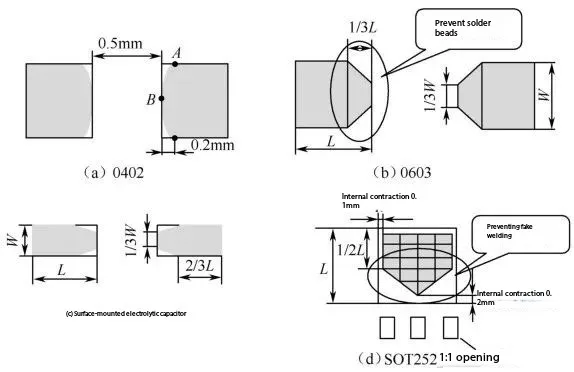
Aperture aspect ratios follow the IPC-7525 golden rule: the optimal range is 1.5:1 para 2:1. When processing 0.5mm pitch QFP components, using an 8-10mil (0.2-0.25milímetros) thick stencil with step-up aperture designs can increase transfer efficiency by 40%.
Area ratio strongly correlates with transfer efficiency (TE):
TE (%) = 100 × (Deposited Paste Volume / Aperture Volume)
Statistical analysis shows that with fixed paste and printing parameters, 95% of TE variation is determined by area ratio. Higher area ratios yield smaller TE deviations and better print volume repeatability.
Advanced Structural Design
Addressing flexible PCB printing sag, UGPCB developed magnetic composite carrier systems with zoned vacuum adsorption, completely resolving thin-board warping. For high-frequency PTFE substrates (por exemplo, Rogers material), added chemical etching post-processing eliminates signal loss from laser burrs.
Step-up stencil technology excels in mixed component height scenarios. Critical design rules must be followed: step edges should maintain a clearance ≥ (1.0mm/1mil)*step height from aperture edges to prevent paste residue.
Breakthroughs in Stencil Manufacturing Processes
Laser Cutting Technology
Modern laser stencils utilize 20μm precision fiber lasers combined with CCD vision systems, achieving full-range accuracy <4μm. UGPCB’s laser platforms feature real-time focal point compensation, ensuring consistency across materials – maintaining 89±1° cut verticality even with Kapton flex materials.
Nano-Coating Innovation
Surface treatment breakthroughs: Nickel-based composite anti-adhesion coatings triple stencil lifespan, extending cleaning cycles from 800 para 5000+ prints. Hydrophilic modified coatings for water-based pastes significantly enhance lead-free solder release, reducing paste residue by 70%.
Material Science Application
UGPCB selects premium 301 aço inoxidável (yield strength >550MPa, surpassing standard 304 steel’s 210MPa). Paired with aerospace-grade aluminum alloy frames (deformation resistance >300N tension), structural stability is maintained even under high-speed printing.
Performance Comparison of Different Stencil Types
| Parâmetro | Laser Stencil | Etched Stencil | Electroformed Stencil |
|---|---|---|---|
| Positioning Accur. | ± 15μm | ± 50μm | ±8μm |
| Min. Aperture | 40μm | 100μm | 30μm |
| Wall Roughness (Rá) | ≤0.8μm | ≥1.5μm | ≤0.5μm |
| Production Lead Time | 4 horas | 8 horas | 24 horas |
| Suitable Components | 01005 to large BGA | ≥0603 | Ultra-fine pitch CSP |
| Cost Effectiveness | ★★★★ | ★★★ | ★★ |
Laser stencils dominate the market due to their precision/cost balance, especially for rapid prototyping. UGPCB offers 4-hour laser stencil turnaround, supporting Gerber X2, ODB++ and 15 other design formats.
How Stencil Properties Impact SMT Printing Defects
Stencil characteristics directly influence seven major SMT printing defects:
-
Thickness Deviation: Causes solder balls, bridging, shorts
-
Aperture Count Errors: Leads to tombstoning, misalignment
-
Positional Tolerance: Results in bridging, misregistration
-
Size Deviation: Causes excessive/insufficient solder
-
Shape Defects: Poor release, pinning
-
Wall Roughness: Increased residue, uneven release
-
Insufficient Cleaning: Clogging, incomplete transfer
Para 0201 componentes, UGPCB employs 30°-45° trapezoidal apertures to suppress pinning. For 0.3mm pitch μBGAs, nano-polishing reduces wall roughness to Ra<0.5μm, garantindo >92% paste release.
Professional Stencil Usage & Maintenance Solutions
Printing Process Optimization
Parameters require dynamic adjustment: Squeegee pressure recommended at 8.4kgf/480mm, separation speed controlled at 1mm/s. For high-density PCBs, a two-step separation technique (0.2mm/s for initial 0.1mm separation, then rapid release) significantly reduces bridging.
Full Lifecycle Management
UGPCB provides a digital twin system with RFID chips tracking:
-
Print Count
-
Tension Degradation Curve
-
Cleaning History
-
Print Quality Correlations
Professional maintenance protocol: Ultrasonic cleaning (ethanol solvent) todo 50 prints, monthly tension checks, quarterly 3D optical aperture inspection.

UGPCB Stencil Technology Advantages Overview
Precision Manufacturing Capabilities
UGPCB operates multi-million dollar laser centers equipped with:
-
Dual-head asynchronous laser cutting
-
In-line 3D white light inspection
-
Automated nano-coating lines
-
Temperature/humidity controlled cleanrooms
Enabling 01005 component stencils (80×150μm apertures) with ±12μm positional accuracy – industry-leading precision.
Intelligent Design Support
AI aperture optimization system automatically identifies risks:
-
Component spacing conflict alerts
-
Auto area ratio calculation
-
Tension simulation
-
Paste rheology modeling
Receive optimization reports within 10 minutes of file upload, eliminating trial-and-error costs.
Sistema de resposta rápida
Global cloud manufacturing network:
-
Asia Hub: 4-hour delivery
-
Europe Hub: 8-hour delivery
-
Americas Hub: 12-hour delivery
Emergency 8/12/24-hour services ensure zero production line downtime.
Critical Stencil Performance Note
Every 5N/cm² decrease in stencil tension increases misregistration probability by 18%. If facing QFN bridging, BGA voiding, or miniature component tombstoning, inspect your stencil condition.
UGPCB engineers master the synergy between stencil design and solder paste rheology. We offer customized solutions for pastes like SAC305 and SnBi57. Contact our technical consultants today for your optimized stencil solution and experience 24-hour rapid prototyping – ensuring precise solder paste deposition for maximum yield.
WeChat
Digitalize o código QR com WeChat