
During a critical Projeto de PCB review, a young engineer defended the reduced silkscreen outline for a BGA chip: “The datasheet specifies 35MIL; we used 25MIL. It’s only 10MIL (0.254milímetros) difference—it should be fine.” The room fell silent. This seemingly minor 10MIL deviation ultimately caused millions in losses due to BGA bridging, scrapping an entire batch of PCB. This article explores the precise physics behind silkscreen design tolerances.
Silkscreen is Not Flat: The Overlooked Third Dimension
PCB silkscreen is more than simple ink markings. Per IPC-4781 standards, cured silkscreen ink forms structures with defined physical heights:
-
Typical Thickness: 2-10 MIL (50.8-254 microns)
-
Common Process Thickness: 4-6 MIL (101.6-152.4 microns)
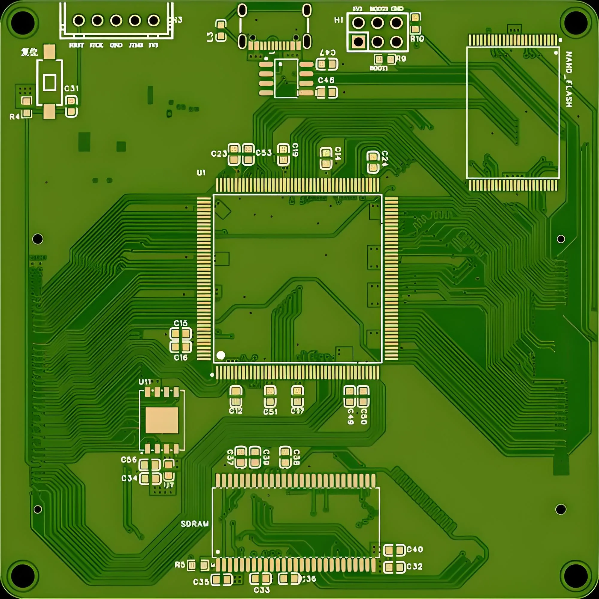
Reducing the BGA silkscreen outline by 10MIL isn’t just a planar reduction. The silkscreen edge physically encroaches onto the pad area, forming a miniature “fence” around each pad. On a 0.8mm pitch BGA, adjacent pad centers are only 31.5MIL apart, with pad diameters typically 12-16MIL. A 10MIL silkscreen encroachment directly threatens the physical space for solder paste flow.
The Fatal Chain Reaction: From Silkscreen Error to BGA Short Circuit
How does silkscreen encroachment trigger soldering failures? Let’s dissect the physical process:
1. Uncontrolled Solder Paste Volume
Estêncil apertures are designed based on PCB pad dimensions. Silkscreen encroachment reduces the usable pad edge area, causing excess solder paste to accumulate within the effective aperture under squeegee pressure. The volume increase (ΔV) can be approximated as:
ΔV ≈ H_silk × L_encroach × S
(Onde: H_silk = Silkscreen thickness, L_encroach = Encroachment length, S = Perimeter of affected pad)
2. Catastrophic Squeeze During Reflow
BGA ball heights are typically 0.3-0.45mm. As the component settles during reflow, excess molten solder paste is violently squeezed in the confined space:
-
Solder from adjacent pads merges.
-
Surface tension fails to retract excess material.
-
Microscopic bridging forms, often invisible to the naked eye.
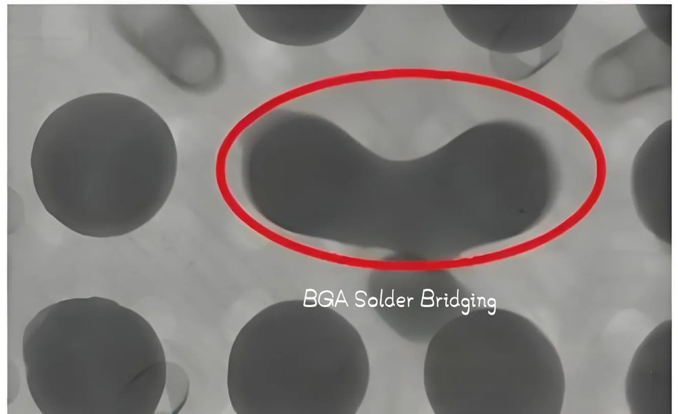
3. Costly Hidden Defects
X-ray inspection reveals that manual visual inspection misses over 95% of bridging defects in BGAs below 0.8mm pitch. These hidden failures cause:
-
Soaring false-pass rates in In-Circuit Testing (TIC).
-
Costly field failures and recalls.
-
Irreparable BGA chip damage from short circuits.
Hard-Won Lessons: Design Rules Forged in Failure
From aerospace to medical electronics, controlling silkscreen on high-density PCBs is now industry-critical:
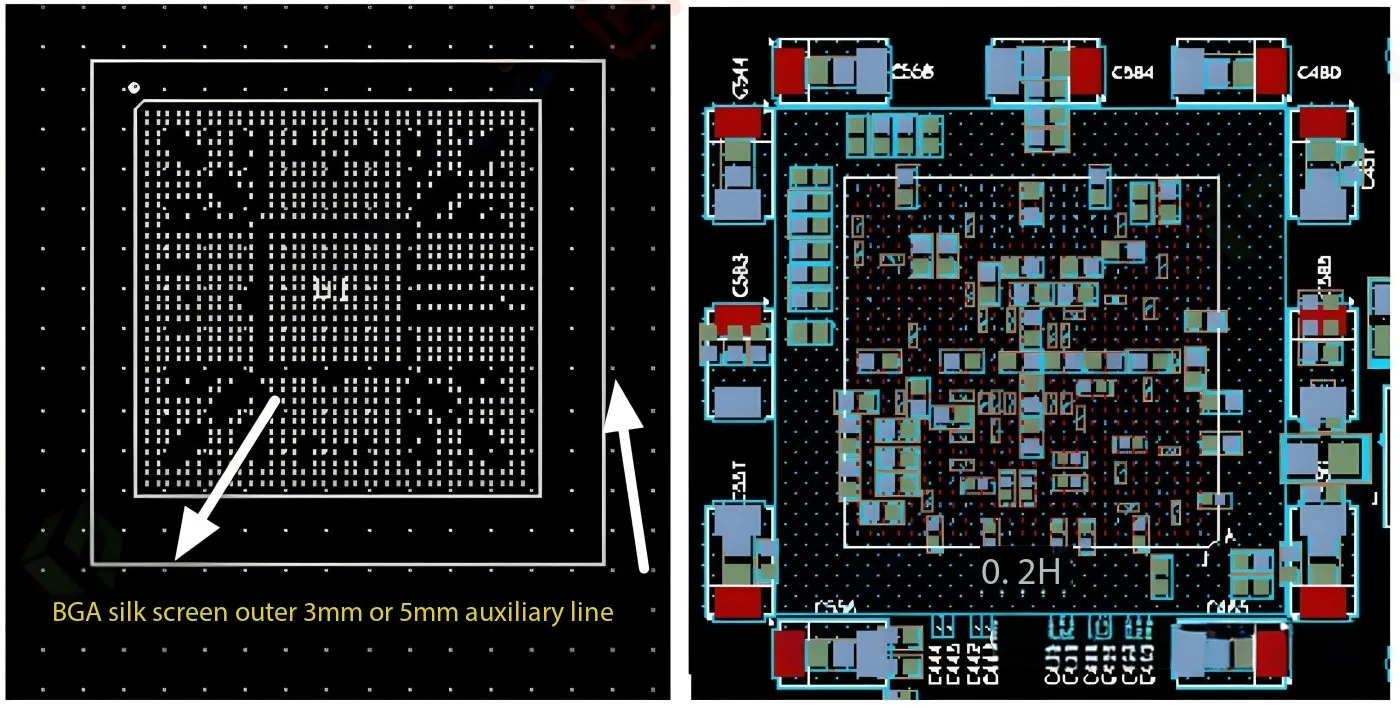
>> Absolute Safety Zone Rule <<<
*Minimum Silkscreen-to-Pad Spacing = Max(0.5milímetros, 3 × Silkscreen Thickness)*
Example: For 125.4μm (6MIL) silkscreen, spacing ≥ 0.5mm (20MIL).
>>> Military-Grade Prevention Strategies <<<
-
Zero Tolerance CAD Libraries: Implement IPC-7351B standard footprint libraries with locked silkscreen outlines.
-
Mandatory DFM Check: Include silkscreen spacing in automated Gerber checks (using Valor, CAM350 rules).
-
3D Solder Paste Simulation: Simulate paste deformation in Cadence Allegro 3D or Zuken CR-8000.
-
First-Article Laser Scan: Measure actual silkscreen height using tools like CyberOptics SE300.
Why Professional PCBA Manufacturers Are Your Last Line of Defense?
When designs carry inherent risks, experienced PCBA partners like UGPCB can mitigate issues through process adjustments:
-
Stencil Laser Cut Compensation: Reduce aperture area by 5-8% in encroached zones.
-
Step Stencil Technology: Use thinner (por exemplo, 15μm reduction) stencil foil in BGA areas.
-
Precision Solder Paste Selection: Use Type #5 powder (20-38μm) for enhanced anti-slump properties.
-
Nitrogen Reflow: Reduce surface tension by ~15% to suppress bridging.
*”68% do 217 silkscreen-related risks intercepted last year involved BGA defects.”*
— UGPCB SMT Factory DFM Report
Action Plan: Upgrade Your Design System Now
Prevent million-dollar losses by implementing these steps immediately:
-
Download IPC-7351B land pattern standards to update component libraries.
-
Enable Silk-to-Pad DRC rules in your EDA tool (set ≥0.2mm).
-
Request precise silkscreen thickness parameters from your PCB supplier for their process.
-
Mandate 3D solder paste simulation for first articles on new projects.
>>> Critical Design Checklist <<<
-
BGA Silkscreen Outline ≥ Datasheet Specified Size.
-
Silkscreen-to-Pad Spacing ≥ 0.5mm.
-
Stencil Files Annotated for Risk Areas.
-
DFM Reports Include Silkscreen Thickness Measurements.
The Secret to Higher Yield Lies in Respecting Every Micron
Para:
-
Obtaining Military-Grade BGA Design Specifications
-
Deep Risk Assessment of Existing Silkscreen Designs
-
Partnering with a Fabricante PCBA Offering Micron-Level Process Control
Contact our technical team immediately for a free DFM audit report and a quote for high-reliability PCBA solutions. We provide end-to-end support from PCB design to volume production, ensuring every BGA joint withstands the toughest demands.
*Observação: Data based on IPC-6012E, IPC-7095C, J-STD-001H standards, and process measurements from UGPCB and multiple EMS providers.*

Itss like you read my mind! You seeem to know so much about this, like you wrote
the book iin it or something. I think that you
could do with some pcs to drive the message home a little bit, but instead of that,
this is fantastic blog. A fantastic read. I’ll definitely be back.
Olá! This bloig post could not be written much better!
Lookin att this article reminds me of my previous roommate!
He continually kept talking about this. I’ll send this information tto him.
Pretty sure he’s going to have a good read. Thankk you for sharing!