
À medida que os dispositivos eletrônicos se tornam cada vez mais sofisticados, uma tecnologia de proteção de ponta derivada de aplicações aeroespaciais está agora salvaguardando a confiabilidade de cada placa de circuito.
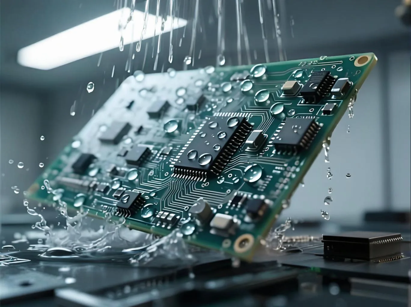
Esta inovação é o Nano-Revestimento de Plasma, também conhecido como Deposição de vapor químico aprimorado por plasma (PECVD). O nano-revestimento é um recurso funcional, flexível, e filme fino em nanoescala caracterizado por suas propriedades hidrofóbicas e oleofóbicas. Utilizando PECVD tecnologia, gases reativos são ativados pelo plasma dentro de uma câmara de vácuo de baixa temperatura, iniciando reações químicas na superfície do substrato para formar uma película protetora semelhante a uma malha com espessura em nanoescala.
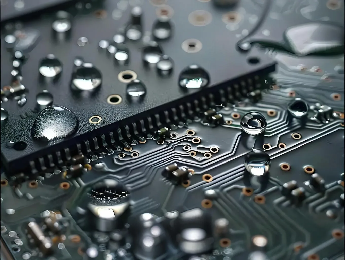
Esta tecnologia não só fornece umidade excepcional, água, e resistência à corrosão para nus PCB e montado Placas de circuito PCBA mas também supera inúmeras limitações associadas aos métodos tradicionais de proteção.
Análise de Princípio Técnico
Nano-revestimento de plasma (PECVD) tecnologia representa uma abordagem avançada para proteção de placas de circuito. Ele emprega plasma para ativar gases reativos em baixa temperatura, ambiente de baixa pressão, formando uma película protetora em nanoescala altamente reticulada.

O núcleo da tecnologia PECVD reside na decomposição de gases reativos em radicais ativos através do plasma. Esses radicais sofrem reações químicas na superfície do substrato, resultando em um ultrafino, revestimento de polímero uniforme.
A temperatura do processo é normalmente baixa, evitando possíveis danos térmicos aos componentes eletrônicos e tornando-o particularmente adequado para montagem completa PCBA placas de circuito.
Em comparação com tecnologias de proteção tradicionais, PECVD permite controle preciso sobre a espessura do revestimento em nanoescala – por exemplo, variando de 15nm a 3000nm – alcançando verdadeira proteção microscópica.
Aplicações de proteção de PCB
Em proteção de PCB nua, nanorrevestimento de plasma demonstra valor único. Devido à sua extrema magreza, o revestimento tem impacto mínimo na correspondência de impedância e na integridade do sinal, garantindo nenhuma interferência com o desempenho do circuito de alta frequência.
Para Interconexão de alta densidade (IDH) Placas, A tecnologia PECVD pode cobrir larguras e espaçamentos de linhas extremamente finos, enfrentando desafios que os materiais de proteção tradicionais não conseguem proteger de forma confiável.
Com uma espessura de revestimento de 15–40 nm, uma classificação de resistência a respingos IPX1–2 pode ser alcançada. Aumentar a espessura para 300–2500 nm permite classificações de proteção contra imersão IPX4–8.
Isto significa que mesmo dispositivos eletrónicos submersos em água durante longos períodos podem ter os seus circuitos centrais protegidos de forma fiável..
Soluções de proteção PCBA
Para placas de circuito PCBA montadas, a tecnologia de nanorrevestimento de plasma se destaca pela cobertura abrangente. Como um processo de deposição em fase gasosa, o revestimento cobre uniformemente todos os cantos do PCBA, incluindo áreas sob componentes, leads de passo fino, e micro-lacunas.
A tecnologia de nanoproteção de plasma da UGPCB é líder neste campo, oferecendo o revestimento conformal mais fino e retrabalhável do setor. Isso permite que os fabricantes reduzam as taxas de refugo e melhorem o rendimento da produção.
Ao contrário dos revestimentos isolantes tradicionais, o nano-revestimento de plasma não forma camadas excessivamente espessas, eliminando a necessidade de mascaramento extenso do conector. Isso agiliza significativamente o processo de produção e reduz os custos de fabricação.
A pesquisa indica que as unidades PCBA com nanorrevestimento de plasma podem reduzir as taxas de reparo de falhas em campo em 40–60%, aumentando significativamente a confiabilidade do produto e reduzindo os custos pós-venda.
Comparação com tecnologias de proteção tradicionais
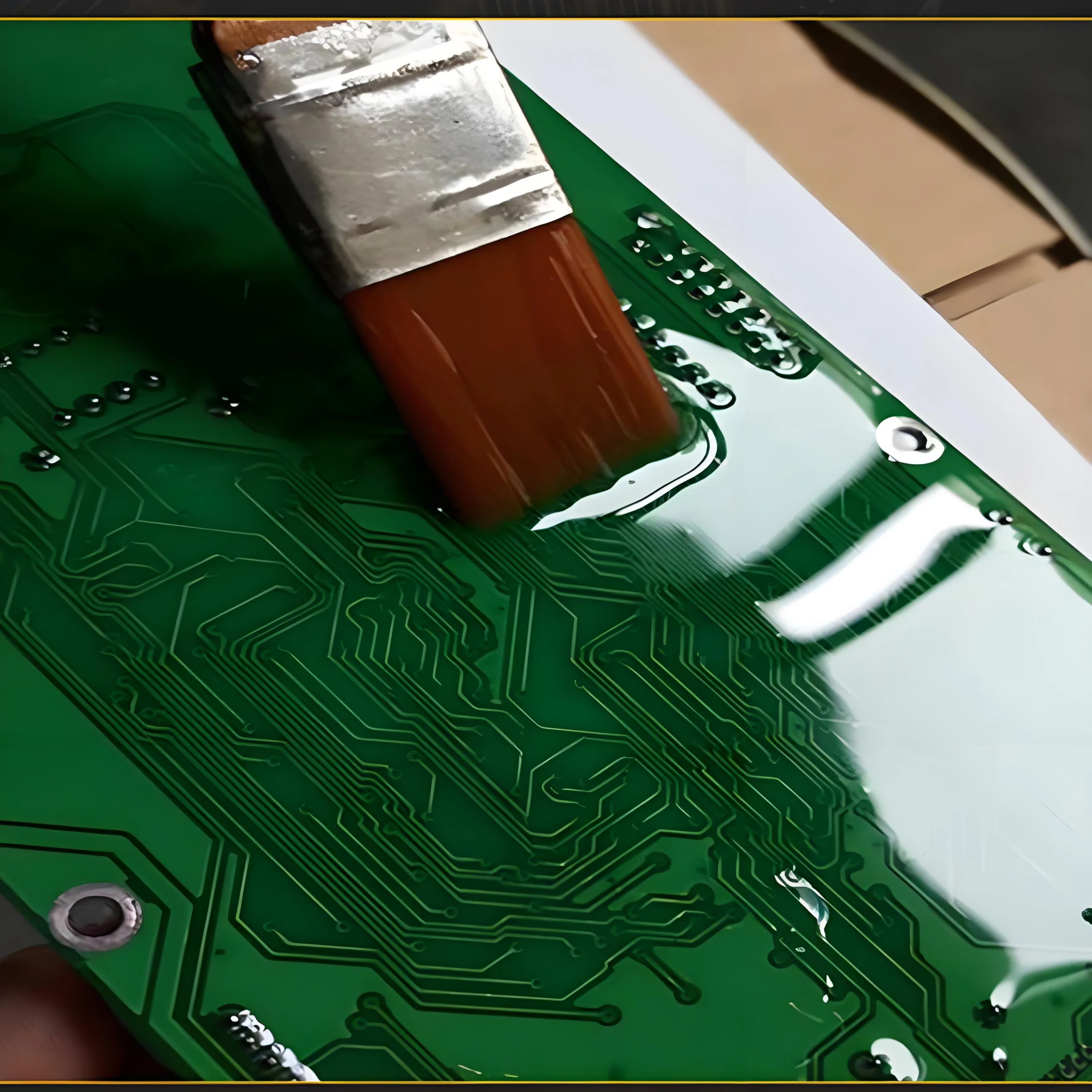
Os métodos tradicionais de proteção de PCB têm várias limitações. Revestimentos isolantes de base líquida são propensos a aplicação irregular, borbulhando, e cobertura incompleta em áreas escondidas. Eles também requerem cura térmica, que emite quantidades significativas de vapores cancerígenos de COV.
Enquanto parileno (poli-p-xilileno) revestimentos oferecem excelente desempenho, eles exigem alto vácuo, ambientes de processamento de alta temperatura, têm baixas taxas de deposição, não são retrabalháveis, e sua espessura pode afetar adversamente a integridade do sinal e o gerenciamento térmico.
Em contraste, a tecnologia de nanorrevestimento de plasma oferece as seguintes vantagens distintas:
-
Revestimento ultrafino: A espessura em nanoescala preserva as características do circuito de alta frequência.
-
Cobertura completa: A deposição em fase gasosa protege todas as superfícies, incluindo áreas escondidas.
-
Segurança ambiental: O revestimento livre de halogênio está em conformidade com as regulamentações ambientais globais.
-
Retrabalhabilidade: Os revestimentos podem ser retrabalhados, minimizando as taxas de sucata.
-
Processo simplificado: Operação automatizada com um toque; o tempo de processamento na câmara é de aproximadamente 0,5–1 hora.
Teste de desempenho e validação de confiabilidade
A confiabilidade dos nanorrevestimentos de plasma foi verificada através de vários testes de envelhecimento acelerado. De acordo com os padrões da indústria, nanorrevestimentos de alta qualidade podem passar em testes de 1.000 horas sob dupla 85 condições (85°C/85% UR) e 1000 ciclos de testes de choque térmico (-40°C a 120 °C), com uma vida útil estimada de 10 a 15 anos.
Teste de estresse altamente acelerado (TEMPO) é um método crítico para avaliar a resistência à umidade de revestimentos protetores. Acelera o envelhecimento do produto através de alta temperatura, alta umidade, e alta pressão para avaliar a confiabilidade dos componentes eletrônicos.
Teste HAST imparcial, normalmente conduzido a 110°C e 85% RH para 264 horas, identifica rapidamente possíveis modos de falha sob revestimentos protetores.
Espectroscopia de Impedância Eletroquímica (EIA) análise mostra que nanorrevestimentos de plasma de alta qualidade mantêm valores de impedância superiores a 1×10⁷ Ω·cm² (no 0.01 hertz) depois 30 dias de imersão em solução de NaCl 0,6M, demonstrando resistência superior à corrosão.
Campos de aplicação e perspectivas de mercado
A tecnologia de nanorrevestimento de plasma é amplamente utilizada em vários setores de produtos eletrônicos:
-
Eletrônica de consumo: Smartphones, notebooks, comprimidos, dispositivos vestíveis
-
Eletrônica automotiva: Unidades de controle do motor, sensores, sistemas de infoentretenimento
-
Dispositivos médicos: Aparelhos auditivos, ventiladores, pipetas, equipamento de monitoramento de pacientes
-
Controles industriais: Drones, fechaduras inteligentes, sensores industriais
-
Aeroespacial: Sistemas aviônicos, eletrônica de satélite
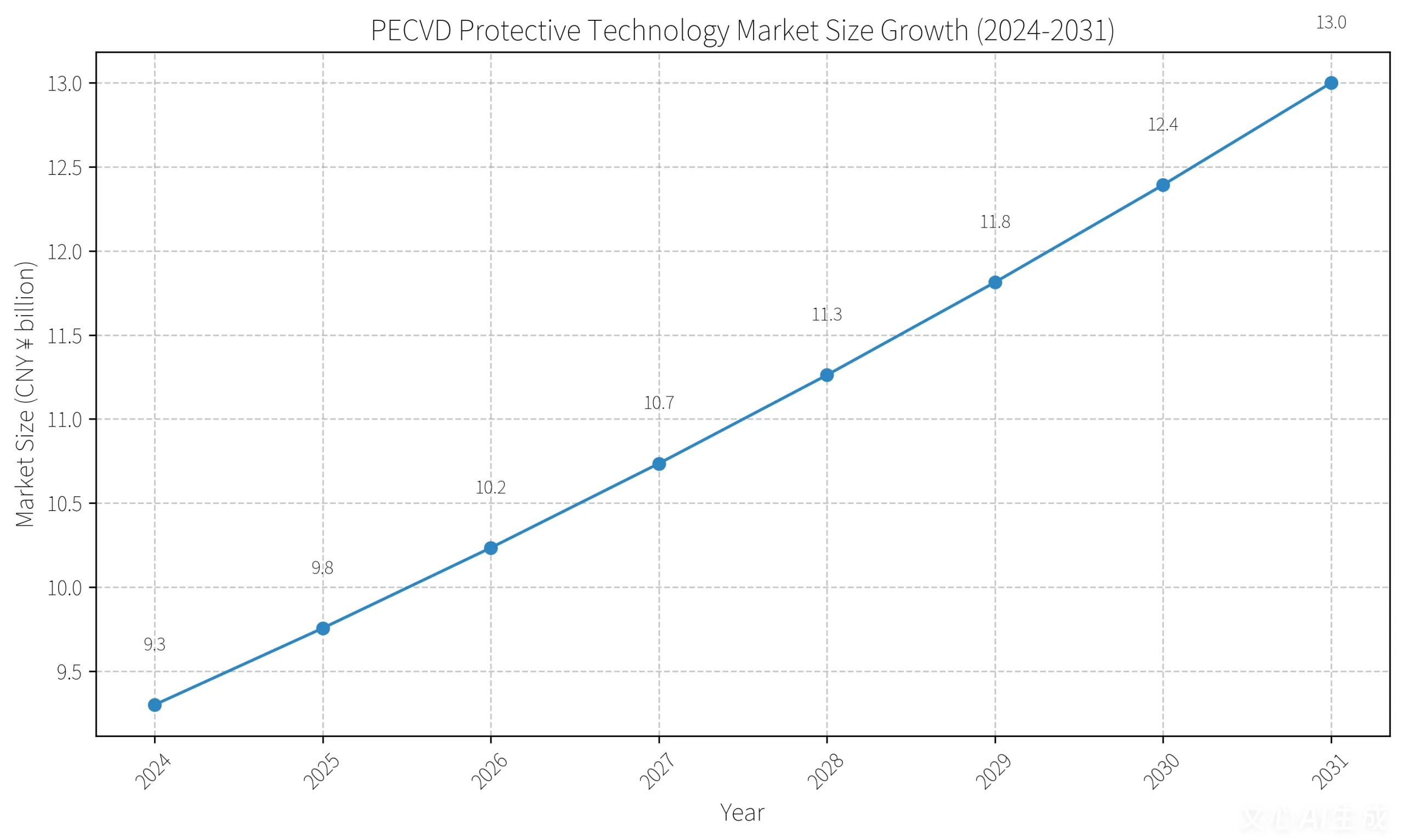
A pesquisa de mercado indica que o mercado global de materiais de proteção para Circuitos Impressos Flexíveis (CPF) sozinho foi de aproximadamente RMB 930 milhões em 2024 e está projetado para atingir quase RMB 1.3 bilhão por 2031, com uma taxa composta de crescimento anual (Cagr) de 4.9%.
Isto reflete o crescimento sustentado do mercado de proteção de dispositivos eletrônicos, com a tecnologia de nanorrevestimento de plasma capturando uma parcela cada vez mais significativa.
Tendências de Desenvolvimento Futuro
A tecnologia de nanorrevestimento de plasma está evoluindo em direção à multifuncionalidade, inteligência, e sustentabilidade ambiental. Novos materiais, como revestimentos aprimorados com grafeno e sistemas de revestimento autocurativos, estão surgindo, oferecendo possibilidades ampliadas para proteção de PCB e PCBA.
A tecnologia de revestimento autocurativo representa outra fronteira. A pesquisa mostra que os revestimentos de vitrímero aprimorados com grafeno podem alcançar reparo de arranhões e recuperação de proteção contra corrosão após aquecimento a 160°C por 3 horas, estendendo significativamente a vida útil protetora efetiva dos produtos.
À medida que os dispositivos eletrônicos continuam a miniaturizar e integrar, com demandas cada vez maiores de confiabilidade, a tecnologia de nanorrevestimento de plasma está definida para se tornar a solução de proteção preferida para eletrônicos de última geração, com sua penetração na fabricação eletrônica aumentando constantemente.
À medida que os dispositivos IoT tendem à miniaturização, a tecnologia de nanorrevestimento de plasma está profundamente integrada à ciência dos materiais e à fabricação inteligente. No futuro, podemos esperar soluções mais inovadoras, como revestimentos autocurativos e fotorresponsivos, introduzir novos paradigmas em proteção eletrônica.
Para fabricantes de eletrônicos que buscam aumentar a confiabilidade dos produtos e a competitividade no mercado, agora é o momento ideal para identificar fornecedores de nanorrevestimento de plasma de alta qualidade e avaliar sua integração nas linhas de produção.

algumas informações muito legais e úteis neste site, também acredito que o design e o estilo possuem recursos maravilhosos.