
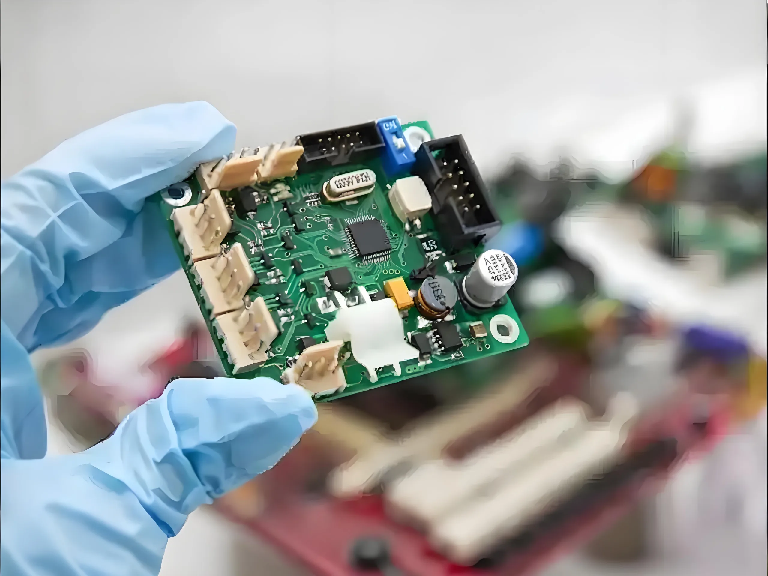
Na fabricação de eletrônicos modernos, defeitos de processo em PCBA (Conjunto da placa de circuito impresso) pode levar à redução da confiabilidade do produto, aumento dos custos de produção, e até falhas de projeto. As estatísticas mostram que os defeitos do processo PCBA são responsáveis por mais de 30% de falhas precoces em produtos eletrônicos, com problemas de juntas de solda e defeitos de revestimento sendo os principais tipos de falha. Este guia abrangente analisa sistematicamente dez defeitos típicos de processo em Fabricação de PCBA- desde rugosidade do revestimento e partículas de cobre até rachaduras nas juntas de solda BGA - e fornece Padrão IPC-compatível, soluções testadas em batalha para ajudar os engenheiros a melhorar a qualidade e a confiabilidade do produto.
1. Rugosidade do Chapeamento: O assassino invisível da uniformidade da superfície
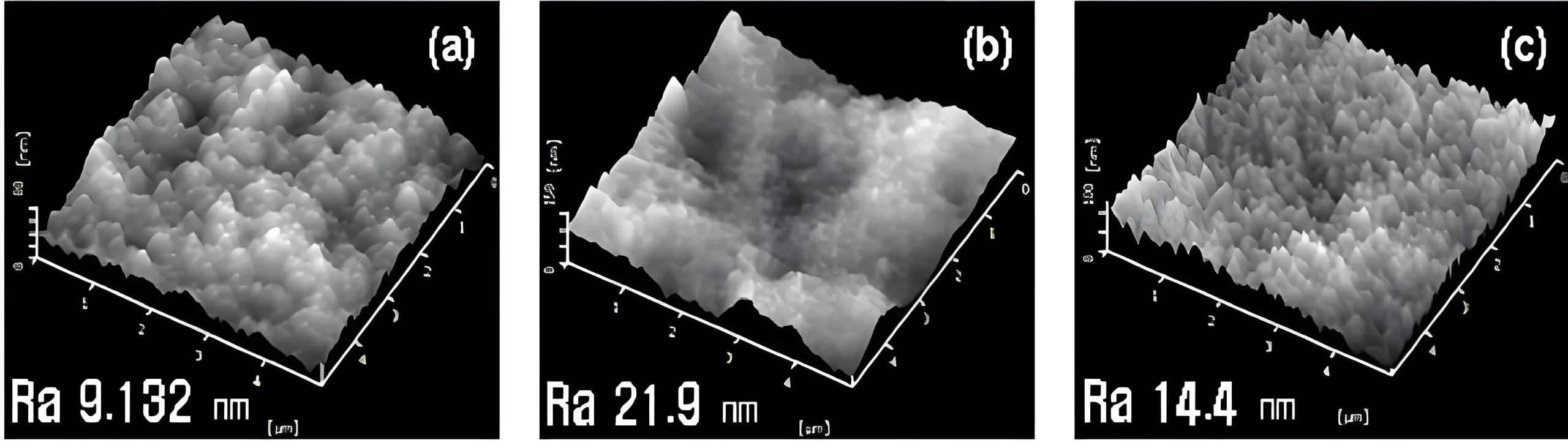
A rugosidade do revestimento é um defeito comum em Fabricação de placas de circuito impresso, caracterizado por bordas ásperas ou uma textura de superfície granular. A rugosidade da borda geralmente decorre de corrente excessiva, causando revestimento irregular, enquanto a rugosidade da placa inteira frequentemente resulta de conteúdo insuficiente de abrilhantador em ambientes de baixa temperatura ou preparação inadequada da placa para retrabalho.
Soluções:
- Ajustar parâmetros de galvanização: Reduza a densidade de corrente e calibre amperímetros para obter uma saída estável.
- Otimize o uso de aditivos: Suplementar branqueadores em baixas temperaturas para melhorar a uniformidade.
- Fortalecer o pré-tratamento: Limpe completamente as placas de retrabalho para remover contaminantes e óxidos.
De acordo com os padrões IPC, PCB de alta qualidade deve manter a tolerância da espessura do cobre ≤5%. A rugosidade do revestimento geralmente excede 10% desvio, impactando criticamente a capacidade de transporte de corrente.
2. Partículas de cobre em superfícies de PCB: Microcontaminação na Cadeia de Processo
Partículas de cobre se manifestam como grãos de cobre aderidos na superfície da placa, provenientes de fontes como alta dureza em água desengordurante alcalina, falhas no sistema de filtragem, ativadores contaminados em revestimento de cobre, ou limpeza incompleta durante a transferência de imagem.
Estratégias de mitigação:
- Melhore a manutenção do filtro: Substitua regularmente os elementos do filtro para manter a limpeza do banho.
- Otimize as sequências de lavagem: Garanta um enxágue completo pós-transferência de imagem e minimize o tempo de armazenamento do painel.
- Monitore os parâmetros do banho: Controle o teor de cobre e a acidez, usando ânodos de cobre fosforado com distribuição uniforme.
3. Chapeamento: O assassino silencioso do revestimento manchado
Os poços de revestimento aparecem como vazios irregulares nas superfícies do PCB, causada por cabides contaminados por limpeza inadequada, equipamento de imagem sem manutenção, ou água dura em processos de pré-revestimento.
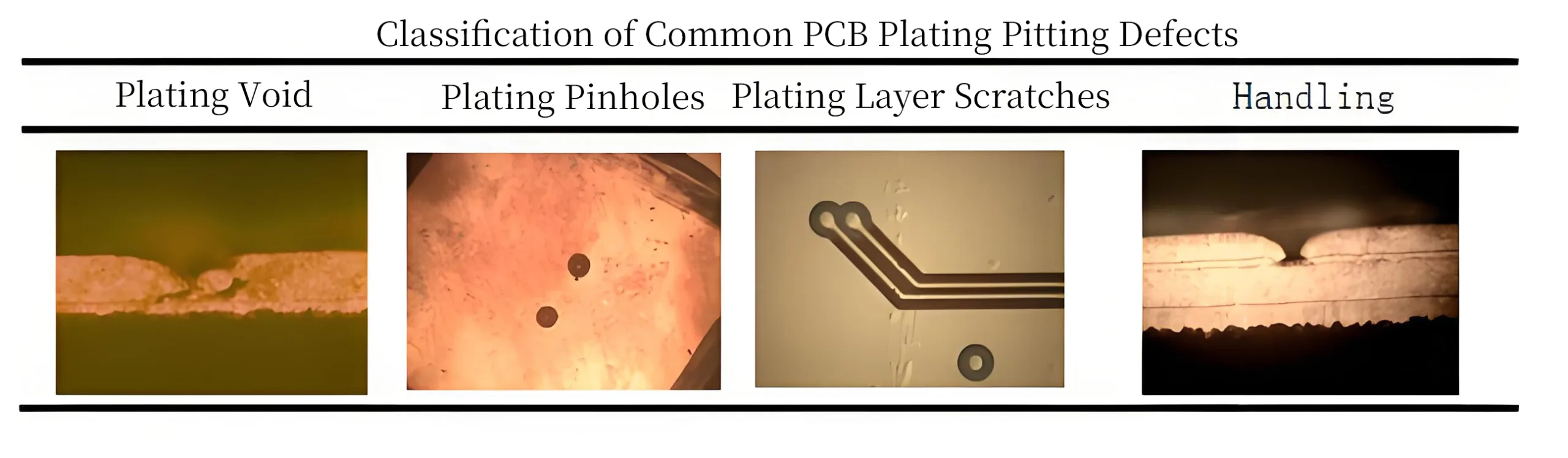
Soluções:
- Implementar protocolos de limpeza profunda para suportes revestidos de cobre.
- Programe manutenção regular para equipamentos de imagem para garantir um desenvolvimento limpo.
- Use água deionizada no pré-revestimento e substitua imediatamente os revestimentos desgastados do suspensor.
4. Branqueamento superficial e inconsistência de cores: Defeitos Visuais com Múltiplas Causas
O badejo da superfície e as variações de cor surgem da agitação irregular do ar, causando variações na espessura do revestimento, bombas de filtro com vazamento, filtros de algodão contaminados, concentrações desequilibradas de micro-condicionante, má qualidade da água, ou conexões anódicas defeituosas.
Medidas de Melhoria:
- Ajuste as posições dos aspersores de ar para agitação uniforme.
- Substitua meios filtrantes qualificados para controlar contaminantes orgânicos.
- Otimize processos de microgravação, melhorar a qualidade da água, e verifique as conexões do ânodo.
Figura: A inspeção de qualidade de placas PCBA sob microscopia de alta ampliação revela rugosidade do revestimento e partículas de cobre – defeitos críticos que requerem atenção.
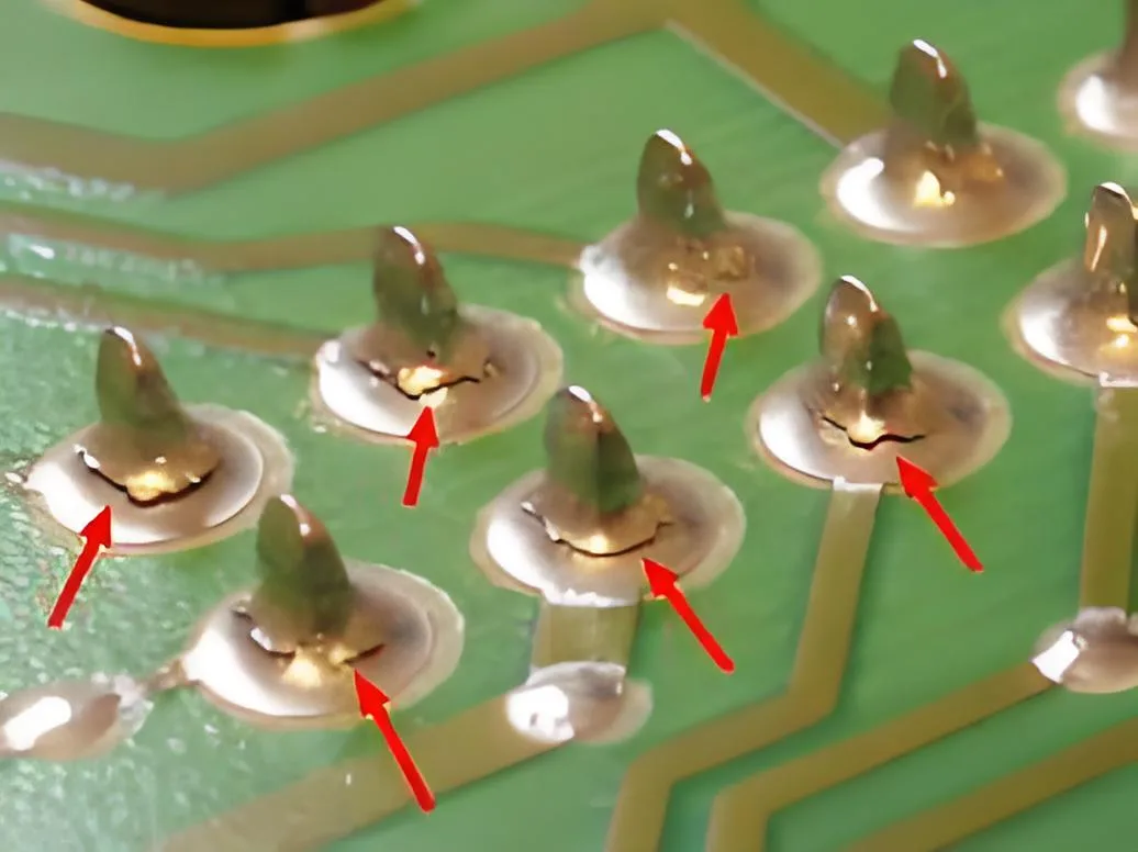
5. Defeitos de soldagem de dispositivos através do orifício: Desafios de confiabilidade
Defeitos de solda THD, como 8.7% solda falsa em placas de controle industriais, decorrem de três questões centrais:
- Fatores materiais: Variações na densidade da fibra de vidro causando distribuição desigual de calor.
- Fatores de processo: Perfil de temperatura inadequado durante retrabalho manual.
- Fatores de projeto: Proporções de aspecto (diâmetro do furo/diâmetro do pino) abaixo do IPC 1.5 recomendação.
Protocolos de otimização:
- Controle dinâmico de temperatura: Ajuste as temperaturas do ferro de solda com base na temperatura de transição vítrea da PCB (Tg).
- Auxiliares de umectação: Use fluxo não limpo com classificação ROL1 com “umedecimento secundário” técnicas.
- Controle de processo: Implemente monitoramento de temperatura em três zonas e rastreabilidade de materiais.
Pós-implementação, as taxas de preenchimento de solda saltaram de 68% para 93%, ciclagem térmica (-40°C~125°C) taxas de aprovação alcançadas 100%, e o tempo de retrabalho caiu de 4.2 para 1.8 minutos por unidade.
6. HDI Blind Via e Falhas de Pad: Riscos de confiabilidade de alta densidade
Placas de IDH aproveite vias cegas e empilhamento de linhas finas para designs compactos, mas introduz riscos como:
- Cego pela confiabilidade: A tolerância de perfuração a laser deve permanecer dentro de ±0,02 mm para evitar desalinhamento.
- Anulação nas paredes do buraco: Desequilíbrios de pH ou ativadores insuficientes durante o revestimento de cobre sem eletrólito.
- Espessura de cobre insuficiente: O IPC exige ≥20μm para paredes de PTH, ainda assim, áreas finas persistem.
Soluções:
- Monitoramento de espessura em tempo real por meio de micrômetros a laser em linha (Tolerância de ±1μm).
- Crie bancos de dados de compatibilidade para sistemas de substrato de fluxo de solda.
- Implante sensores ambientais (temperatura/umidade/COV) com limites de alerta automático.
7. Defeitos na borda do processo: Fontes subestimadas de reações em cadeia
Defeitos de borda (rebarbas, furos de ferramentas desalinhados, delaminação) elevar as taxas gerais de defeitos 10-15%. As médias da indústria mostram 2.2% taxas de defeito para problemas relacionados à borda, com consequências incluindo:
- Desalinhamento do furo da ferramenta >0.1mm reduzindo SMT precisão de posicionamento de 0,2 mm (padrão: 0.1milímetros).
- Delaminação das bordas enfraquecendo a integridade estrutural por 30% e aumentando a atenuação do sinal 15-20%.
- Rebarbas causando riscos de ponte de solda e danificando os bicos pick-and-place.
Sistema de Controle Holístico da UGPCB:
- Alívio do estresse: Aclimatar os substratos a 25±1°C/50±5% UR para 12 horas.
- Perfuração de precisão: 0.003máquinas com precisão de mm com bancos de dados de velocidade de espessura.
- Rastreabilidade total: Integração MES para rastreamento de defeitos em tempo real.
Essas medidas reduziram as taxas de defeitos nas bordas para <0.1%, muito abaixo do 2.2% Média da indústria.
Figura: A microscopia de defeitos nas bordas revela desalinhamento de ferramentas e rebarbas que afetam a precisão do SMT.
8. Rachaduras nas juntas de solda e quedas de componentes: Falhas Duplas no Processo de Material
Quebra de junta de solda, um defeito crítico de PCBA, frequentemente rastreia a corrosão da camada de níquel durante o revestimento ENIG. O níquel oxidado forma IMCs não uniformes com solda, levando a rachaduras na interface IMC-níquel.
Melhorias de processo:
- Controle de fósforo: Reduza a vida útil do banho de níquel sem eletrólito para aumentar o fósforo (faixa de alto P).
- Espessura do níquel: Mantenha ≥4μm para minimizar corrosão.
- Espessura do ouro: Limite a ≤0,1μm com tempo de imersão reduzido.
9. Falhas nas juntas de solda BGA: Microfissuras e Concentração de Tensão
Articulações BGA (0.4passo mm, 0.2mm altura) são propensos a microfissuras sob vibração ou choque térmico. Um servidor IDH caso mostrado 300% aumento de resistência testes pós-vibração.
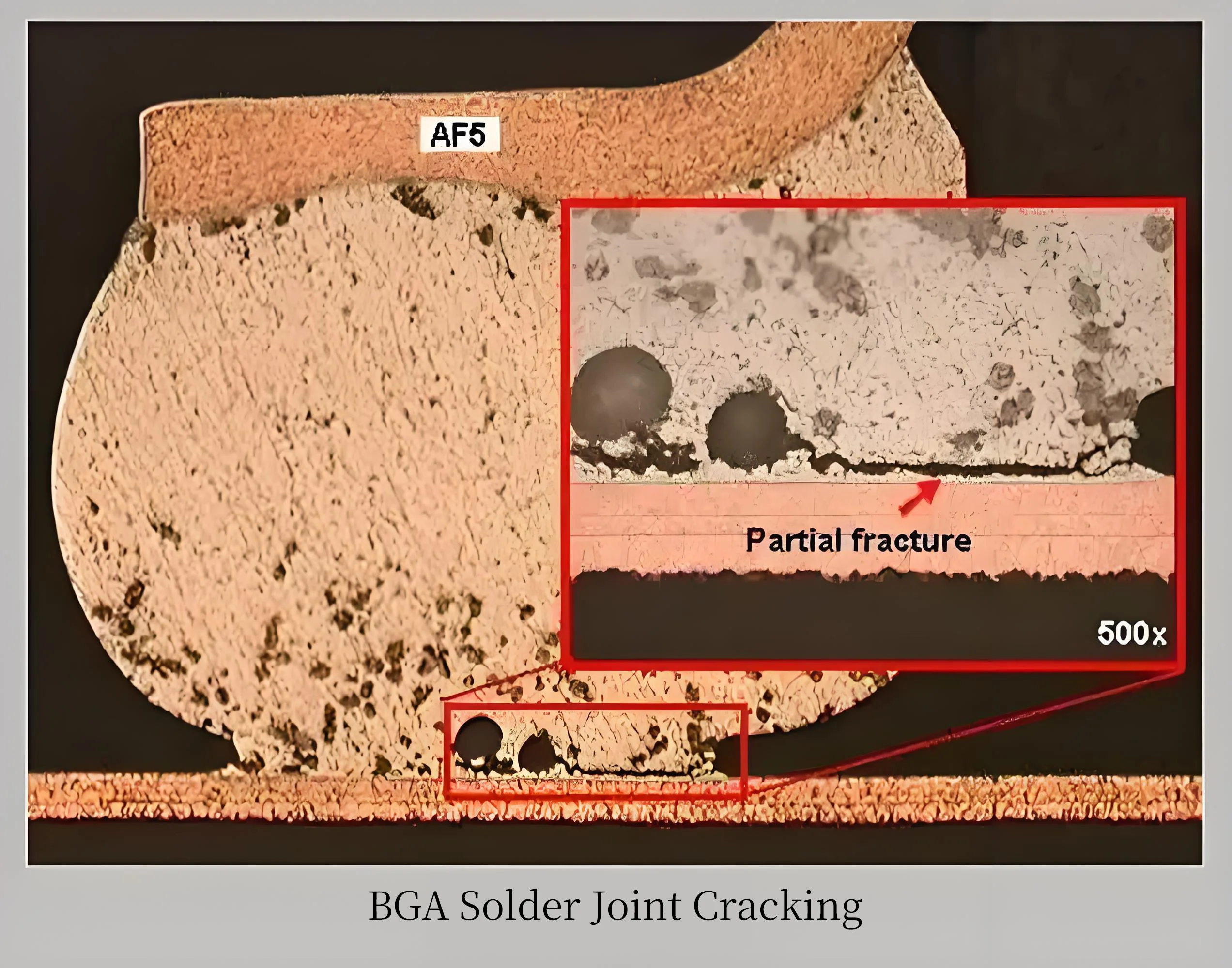
Soluções:
- Otimização de layout: Evite a colocação inadequada dos parafusos do dissipador de calor, tensionando os BGAs.
- Controle de flexão: Minimize a flexão repetida para evitar o levantamento da almofada.
- Correspondência de materiais: Selecione substratos/solda com CTE correspondente (por exemplo, FR-4 de alta Tg a 8 ppm/°C vs.. padrão 15ppm/°C).
10. Design térmico inadequado: Crise de componentes sob alta temperatura
Falha de componente induzida termicamente é comum. Um patenteado “PCB cego com dissipador de calor integrado” melhora o desempenho térmico através de cavidades internas e dissipadores de calor de alta eficiência, dissipando rapidamente o calor e reduzindo os riscos de danos térmicos.
Recursos de design inovadores:
- As cavidades de calor aumentam a transferência térmica do coletor para a placa e o resfriamento geral.
- Os dissipadores de calor absorvem e difundem o calor do PCB, com fluxo de ar transferindo eficientemente o calor.
Tabela resumida para referência:
| Tipo de defeito | Média da indústria. | Taxa melhorada | Parâmetros de controle chave |
|---|---|---|---|
| Defeitos de borda | 2.2% | 0.1% | Precisão da broca 0,003 mm, 12h aclimatação |
| Solda Falsa THD | 8.7% | 0.9% | Proporção de aspecto ≥1,5, controle de temperatura de três zonas |
| Furo de parede de cobre | – | IPC ≥20μm | Tolerância de espessura ±1μm |
| Taxa de preenchimento de solda | 68% | 93% | Perfil dinâmico: 280°C/3s + 380°C/2s |
O controle e a prevenção sistemáticos do processo podem mitigar a maioria dos defeitos do PCBA. A parceria com fornecedores experientes e a implementação de sistemas de qualidade robustos são essenciais para aumentar a confiabilidade do PCBA. Para soluções PCBA de alta confiabilidade e consultas técnicas, contato nós hoje.

algumas informações realmente interessantes , bem escrito e amplamente amigável ao usuário.