

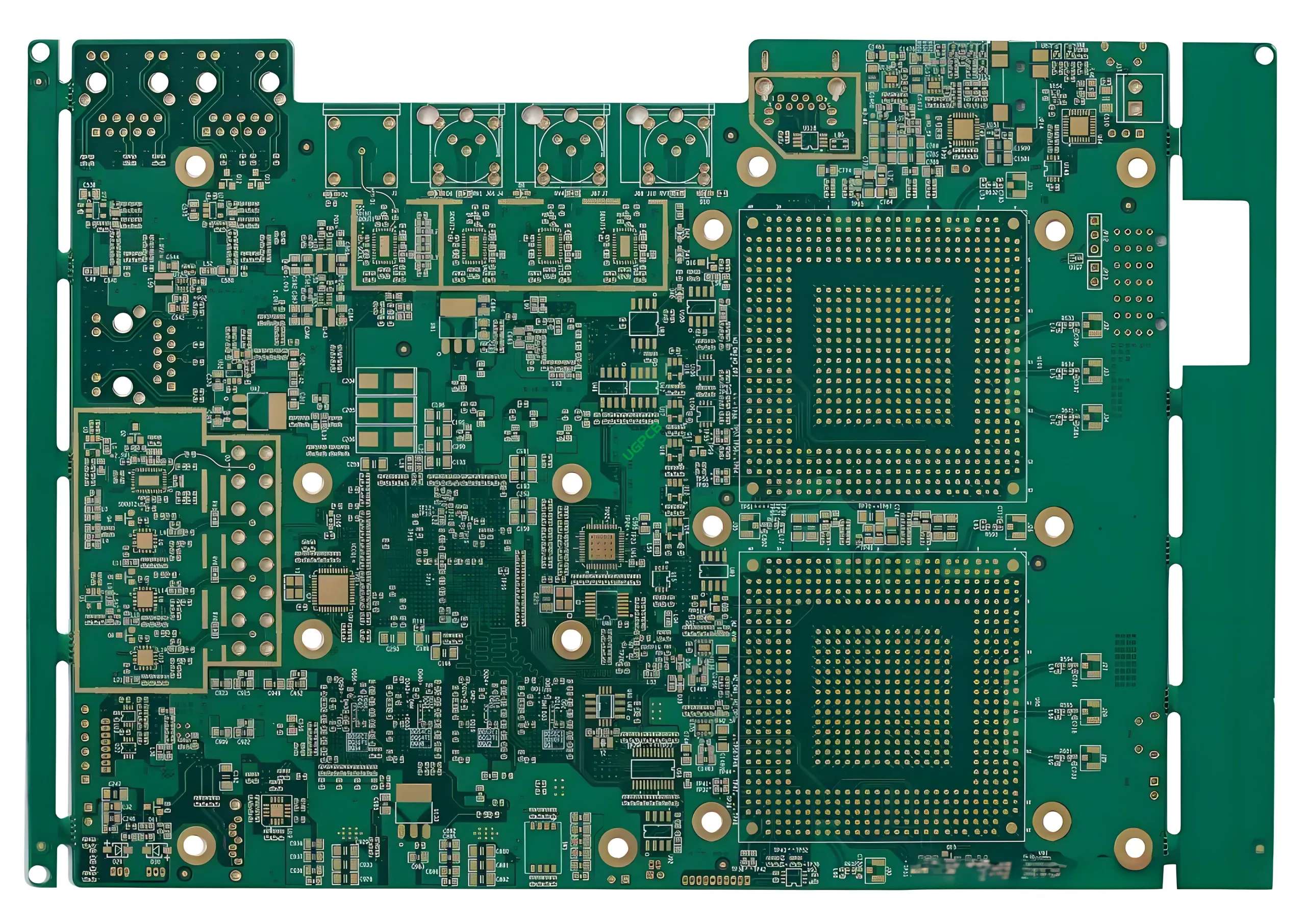
What is a BGA PCB?
A Ball Grid Array (BGA) แผงวงจรพิมพ์ (พีซีบี) is a type of แผงวงจร that features a grid of solder balls on its underside, used for connecting ส่วนประกอบอิเล็กทรอนิกส์ to the board. This design allows for higher input/output connection density and improved electrical performance compared to traditional through-hole or surface-mount technology (SMT) PCBS.
ข้อกำหนดการออกแบบ
Designing a BGA PCB involves several key considerations:
- วัสดุ: Typically made from FR-4, วัสดุคอมโพสิตที่รู้จักกันดีในเรื่องคุณสมบัติทางไฟฟ้าที่ยอดเยี่ยมและความสามารถในการจ่ายได้.
- จำนวนเลเยอร์: Multilayer designs are common, providing more space for complex circuitry.
- ความหนาของทองแดง: Generally specified as 1/1OZ, balancing conductivity with cost-effectiveness.
- การรักษาพื้นผิว: Often includes immersion gold to enhance solderability and protect against oxidation.
- ติดตามและพื้นที่: Minimum trace and space are typically set at 4mil, อนุญาตให้มีรายละเอียดที่ดีในการออกแบบวงจร.
มันทำงานอย่างไร?
The BGA PCB functions by providing a platform where electronic components can be mounted and interconnected using a grid of solder balls. These balls are aligned in a pattern on the underside of the board, corresponding to contact pads on the component. When heat is applied, the solder melts and creates a strong bond, ensuring reliable electrical connections.
การใช้งาน
Due to their high density and reliability, BGA PCBs are widely used in various electronic products including:
- Computer motherboards
- High-performance servers
- อุปกรณ์เครือข่าย
- Advanced consumer electronics like gaming consoles and smart devices
การจำแนกประเภท
BGA PCBs can be classified based on several factors:
- โดยวัสดุ: ส่วนใหญ่ทำจาก FR-4 เนื่องจากความสมดุลของต้นทุน, ความแข็งแกร่ง, และคุณสมบัติไฟฟ้า.
- โดยการนับเลเยอร์: Can range from double-sided to multilayer configurations, ขึ้นอยู่กับความซับซ้อนของวงจร.
- โดยการรักษาพื้นผิว: ตัวเลือกรวมถึงการแช่ทองคำ, hasl, or organic solderability preservatives (โอป), แต่ละเสนอการป้องกันและการประสานในระดับที่แตกต่างกัน.
วัสดุที่ใช้
The primary วัสดุ used in manufacturing BGA PCBs include:
- FR-4: ลามิเนตอีพ็อกซี่เสริมแก้วที่ให้ความแข็งแรงเชิงกลที่ยอดเยี่ยมและความเสถียรทางความร้อน.
- ทองแดง: ใช้สำหรับชั้นนำไฟฟ้า, ด้วยความหนาแตกต่างกันไปตามข้อกำหนดการออกแบบ.
- หน้ากากบัดกรี: Typically green or white, ช่วยปกป้องร่องรอยทองแดงจากการออกซิเดชั่นและการลัดวงจรโดยไม่ตั้งใจ.
- ทองแช่: A surface treatment that improves solderability and protects against corrosion.
ลักษณะประสิทธิภาพ
Key performance attributes of a BGA PCB include:
- ความหนาแน่นสูง: ช่วยให้มีส่วนประกอบมากขึ้นบรรจุในพื้นที่เล็ก ๆ.
- ความน่าเชื่อถือ: The use of solder balls reduces the risk of mechanical failure due to vibration or impact.
- ความสมบูรณ์ของสัญญาณ: ปรับปรุงเนื่องจากเส้นทางสัญญาณที่สั้นลงและลดการตัดไม้.
องค์ประกอบเชิงโครงสร้าง
ตามโครงสร้าง, a BGA PCB comprises:
- ชั้นนำไฟฟ้า: ทำจากทองแดง, สลักลงในรูปแบบวงจรที่ต้องการ.
- เลเยอร์ฉนวน: ป้องกันกางเกงขาสั้นไฟฟ้าระหว่างชั้นนำไฟฟ้า.
- Solder Balls: Arranged in a grid pattern on the underside of the board for component attachment.
คุณสมบัติที่โดดเด่น
Some notable features of a BGA PCB are:
- สนามที่ดี: ช่วยให้เชื่อมต่อระหว่างกันที่มีความหนาแน่นสูง, ทำให้เหมาะสำหรับอุปกรณ์ขนาดกะทัดรัด.
- ความทนทาน: The use of solder balls provides a strong mechanical bond between the board and components.
- ความอเนกประสงค์: เหมาะสำหรับแอปพลิเคชันที่หลากหลายเนื่องจากการนับเลเยอร์ที่ปรับแต่งได้และตัวเลือกวัสดุ.
กระบวนการผลิต
The manufacturing process of a BGA PCB involves several steps:
- การออกแบบและเค้าโครง: การใช้ซอฟต์แวร์พิเศษเพื่อสร้างรูปแบบวงจร.
- การเตรียมวัสดุ: การตัดวัสดุฐานเป็นขนาดและพื้นผิวการทำความสะอาด.
- การเคลือบ: การซ้อนและเชื่อมแต่ละชั้นภายใต้ความร้อนและความดัน.
- การแกะสลัก: การลบทองแดงส่วนเกินเพื่อสร้างเส้นทางวงจรที่ต้องการ.
- การชุบ: การเพิ่มชั้นโลหะบาง ๆ ลงใน Vias และพื้นที่ทองแดงที่เปิดเผย.
- แอปพลิเคชันมาสก์ประสาน: Applying the green or white coating to protect traces.
- การรักษาพื้นผิว: Applying immersion gold or other treatments for solderability.
- การตรวจสอบขั้นสุดท้าย: สร้างความมั่นใจในคุณภาพและการใช้งานก่อนการจัดส่ง.
ใช้เคส
Common scenarios where a BGA PCB might be employed include:
- แอพพลิเคชั่นเชื่อมต่อระหว่างกันที่มีความหนาแน่นสูงในอุปกรณ์มือถือ.
- ระบบการสื่อสารขั้นสูงที่ต้องการการสูญเสียสัญญาณต่ำ.
- เครื่องมือทางการแพทย์แบบพกพาที่ต้องการประสิทธิภาพที่เชื่อถือได้ในสภาพแวดล้อมที่รุนแรง.
- ยานยนต์อิเล็กทรอนิกส์ที่ต้องการความแข็งแกร่งและอายุยืน.
โดยสรุป, the BGA PCB represents a significant advancement in printed circuit board technology, นำเสนอความซับซ้อนและประสิทธิภาพที่เหนือชั้นสำหรับการใช้งานอิเล็กทรอนิกส์ที่ทันสมัย. Its design flexibility, combined with superior signal integrity and durability, makes it an essential component in the development of next-generation electronic products and beyond


