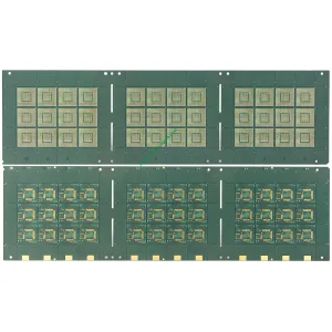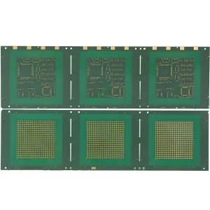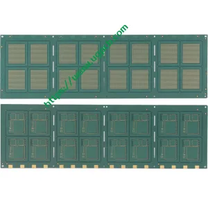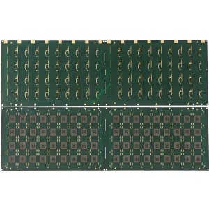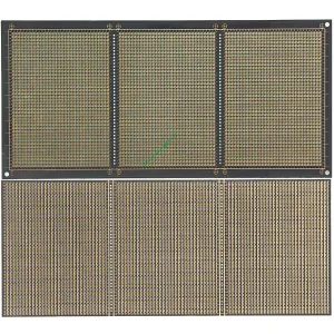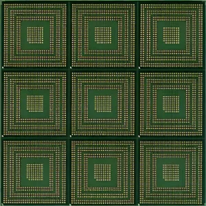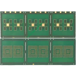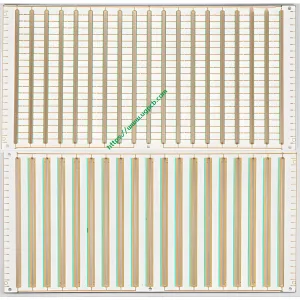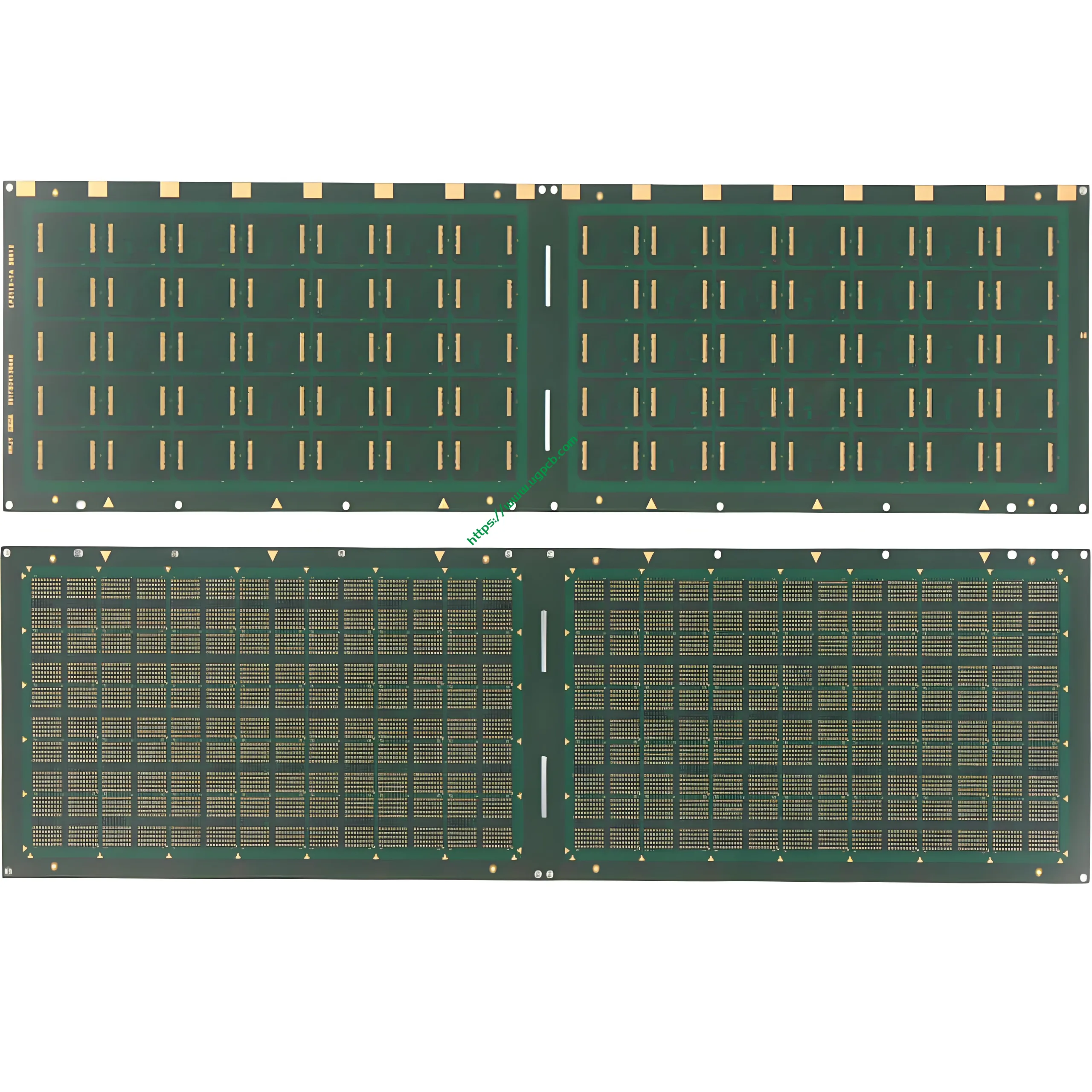
Lead the High-Speed Era: UGPCB’s 4-Layer DDR Substrate Board – The Superior Interconnect Solution for Your Core ICs
In the booming landscape of high-performance computing, الذكاء الاصطناعي, and next-generation communication devices, every advancement in Double Data Rate (نزع السلاح والتسريح وإعادة الإدماج) technology places stricter demands on PCB substrates. الاستفادة من الخبرة العميقة في high-end PCB manufacturing و الركيزة IC الحلول, UGPCB introduces its premium 4-Layer DDR Substrate Board. Engineered with cutting-edge materials, it is specifically designed to carry high-performance memory chips (على سبيل المثال, DDR4, DDR5, LPDDR), serving as your reliable partner in the pursuit of ultimate speed and stability.
نظرة عامة على المنتج & تعريف
أ 4-Layer DDR Substrate Board is a High-Density Interconnect (مؤشر التنمية البشرية) printed circuit board designed for packaging and connecting Dynamic Random-Access Memory (نزع السلاح والتسريح وإعادة الإدماج) رقائق. It acts as a critical bridge between the chip and the mainboard, responsible for transmitting high-speed signals, distributing power, and providing stable mechanical support. على عكس المعيار لوحات ثنائي الفينيل متعدد الكلور, DDR substrates demand near-perfect signal integrity, الإدارة الحرارية, and dimensional accuracy. This product from UGPCB is tailor-made to meet these stringent requirements.
اعتبارات التصميم الحرجة
-
التحكم الدقيق في المعاوقة: Paramount for DDR PCB design, it minimizes signal reflection and distortion during high-speed data transmission.
-
نزاهة السلطة (باي): Dedicated power and ground plane design ensures clean, stable power delivery, reducing noise interference on critical signals.
-
سلامة الإشارة (و): Optimized routing using microstrip and stripline structures minimizes crosstalk and delay, forming the foundation for stable performance post-تجميع PCBA.
-
-
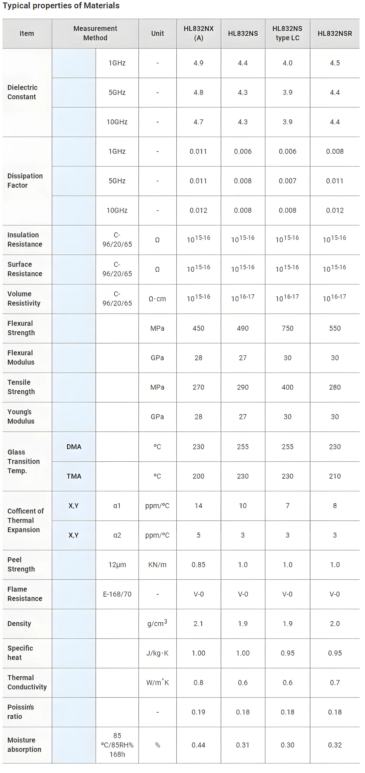
الإدارة الحرارية: The substrate material must exhibit excellent thermal properties to aid chip dissipation and ensure long-term reliability.
كيف يعمل
The 4-Layer DDR Substrate connects the hundreds of micro-pins of a memory chip to the corresponding motherboard circuits via its precise internal layers. إنه “شطيرة” كومة المتابعة (إشارة-أرض-قوة-إشارة) provides clear return paths for high-speed signals, effectively suppressing Electromagnetic Interference (emi). The soft gold surface finish ensures a reliable, low-resistance solder joint with the chip’s solder balls (على سبيل المثال, in BGA packages).
التطبيقات الأولية & تصنيف
-
التطبيقات الأولية: Extensively used in servers, مفاتيح مركز البيانات, high-end GPUs, بطاقات تسريع الذكاء الاصطناعي, network storage devices, and any cutting-edge electronic product requiring high-speed, high-capacity memory.
-
تصنيف:
-
حسب عدد الطبقات: Beyond standard 4-layer, designs can extend to 6, 8, or more layers based on complexity.
-
حسب المادة: Can be categorized into standard FR-4, Mid-Loss, and this product’s focus – Low-Loss material substrates.
-
مواد & مواصفات الأداء
| المعلمة | مواصفة | ميزة الأداء |
|---|---|---|
| المواد الأساسية | Mitsubishi Gas Chemical HL832 | Industry-recognized, عالية الأداء, low-loss (Low Df) laminate designed for high-speed digital circuits, significantly reducing signal transmission loss. |
| عدد الطبقة | 4 طبقات | أفضل “إشارة-أرض-قوة-إشارة” كومة المتابعة, balancing design complexity, يكلف, والأداء. |
| سمك الانتهاء | 0.25مم | Ultra-thin profile, conforming to compact chip packaging trends for integration into miniaturized devices. |
| سمك النحاس | 0.5أوقية (17.5ميكرومتر) | Standard starting weight, suitable for fine-line etching; can be plated up for higher current needs. |
| لون قناع اللحام | أخضر (AUS308) | Provides excellent insulation protection and visual contrast for Optical Inspection (الهيئة العربية للتصنيع) بعد تجميع ثنائي الفينيل متعدد الكلور. |
| الانتهاء من السطح | الذهب الناعم (يوافق) | Excellent surface planarity and low hardness, ensures superior compatibility with wire bonding or BGA solder balls for reliable connections. |
| Minimum Drilled Hole Size | 100ميكرومتر | Supports high-density micro-via design for complex chip pinout interconnection. |
| دقيقة. عرض الخط/المساحة | 50ميكرومتر / 75ميكرومتر | High-precision routing capability allows more high-speed lines in limited space, مقابلة ربط ثنائي الفينيل متعدد الكلور عالي الكثافة design needs. |
هيكل المنتج & الميزات الرئيسية
-
بناء: Typical 4-layer sequential lamination: الطبقة العليا (Signal/Components) -> الطبقة الداخلية 1 (Solid Ground Plane) -> الطبقة الداخلية 2 (Solid Power Plane) -> الطبقة السفلية (Signal/Components). This structure offers optimal shielding for high-speed signals.
-
الميزات الرئيسية:
-
Superior High-Speed Performance: HL832 low-loss material ensures excellent signal integrity for high-frequency DDR signals.
-
High-Density Interconnect Capability: 100μm micro-vias and 50μm line width technology support advanced chip packaging.
-
موثوقية عالية: ENIG surface finish offers excellent solderability and oxidation resistance for long-term stability.
-
Ultra-Thin & دقيق: 0.25mm overall thickness meets stringent space requirements in modern electronics.
-
 عملية التصنيع الدقيقة
ملكنا تصنيع ثنائي الفينيل متعدد الكلور process adheres to the highest quality standards:
Material Prep → Inner Layer Imaging & Etching → Lamination & Drilling → Metallization & Plating → Outer Layer Imaging → Surface Finish (يوافق) → Solder Mask Application → Profiling → Electrical Test & التفتيش النهائي.
Each stage is supported by advanced inspection equipment (على سبيل المثال, الهيئة العربية للتصنيع, اختبار مسبار الطيران), ensuring every الركيزة IC delivered is flawless.
حالات الاستخدام النموذجية
This 4-Layer DDR Substrate is the ideal choice for:
-
مراكز البيانات & الخوادم: Carrying CPU and memory modules for massive data processing.
-
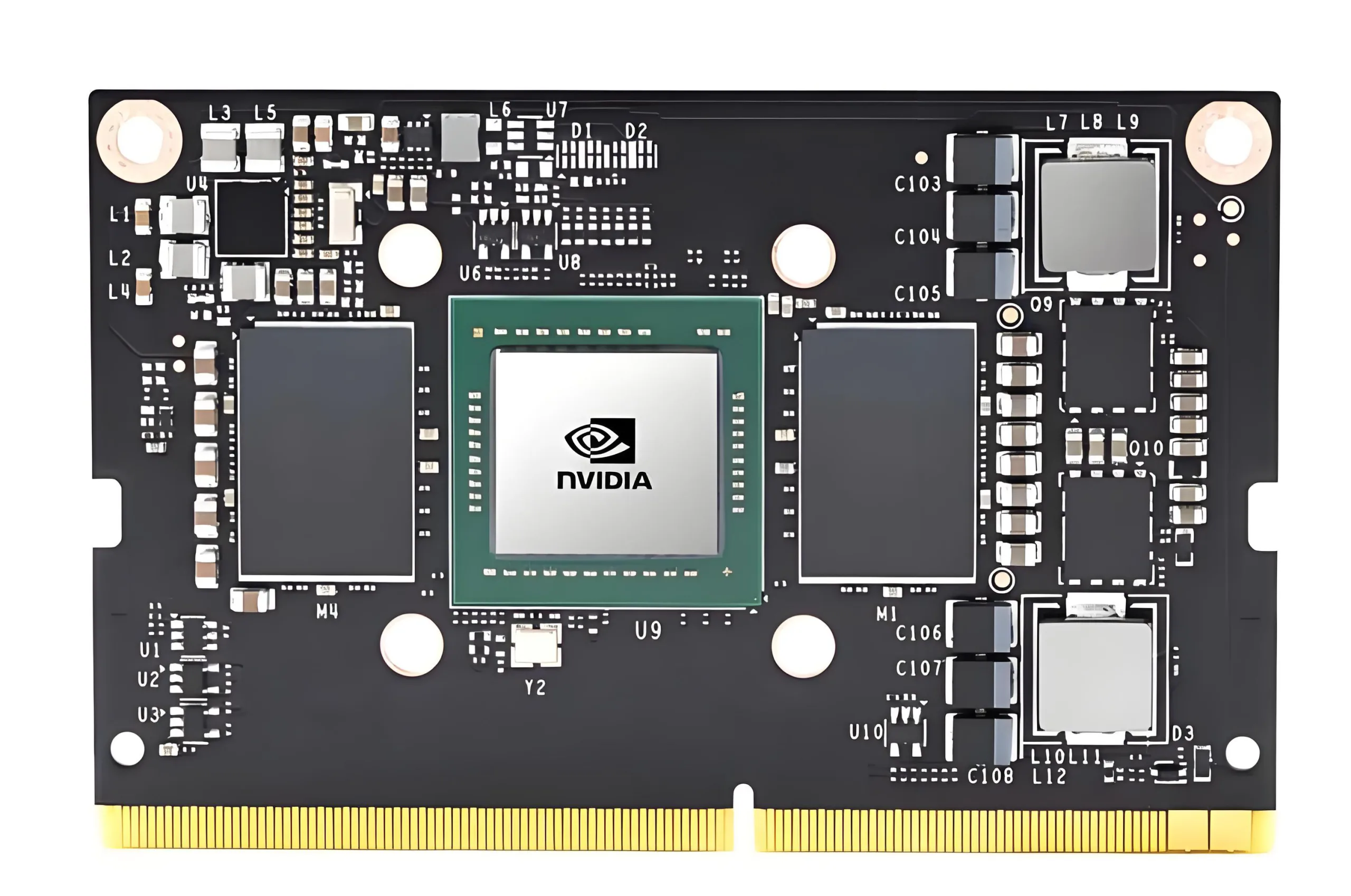
منظمة العفو الدولية & Machine Learning Hardware: Memory subsystems in GPU, NPU accelerator cards.
-
معدات الاتصالات المتطورة: High-speed memory units in 5G base stations and core network gear.
-
الإلكترونيات الاستهلاكية الرائدة: Main memory substrates in top-tier gaming consoles and laptops.
Why Choose UGPCB’s 4-Layer DDR Substrate?
نحن أكثر من أ الشركة المصنعة لثنائي الفينيل متعدد الكلور; we are your solution provider for high-speed design challenges. With a dedicated دعم تصميم ثنائي الفينيل متعدد الكلور team, proven capabilities in multilayer PCB prototyping and mass production, and a deep understanding of signal integrity engineering, choosing UGPCB means gaining not just a high-quality substrate, but an accelerator for your product’s success.
Contact our expert team today for a project-specific quote and technical consultation. Power up your high-speed design with UGPCB!