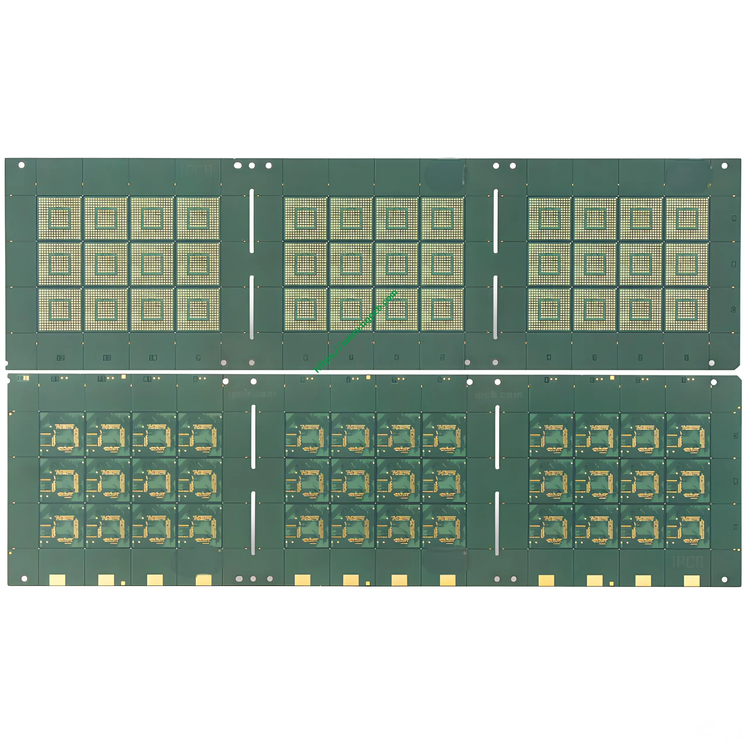
High-Performance BGA IC Substrate: The Precision Foundation for Advanced IC Packaging
In the era of smaller, أسرع, and more powerful electronics, advanced IC packaging is critical. Acting as the essential interface between the silicon die and the main لوحة الدوائر المطبوعة (ثنائي الفينيل متعدد الكلور), ال BGA IC Substrate is the core component of high-end semiconductor packages. UGPCB leverages deep تصنيع ثنائي الفينيل متعدد الكلور expertise and advanced processes to deliver high-performance, موثوق BGA package substrate الحلول.
1. What is a BGA IC Substrate?
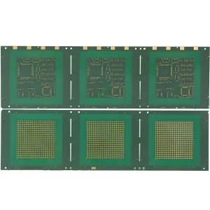
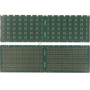
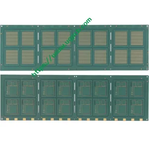
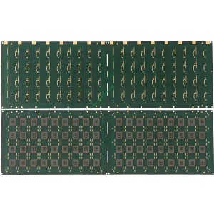
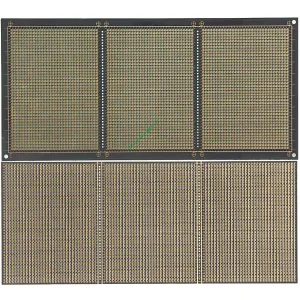
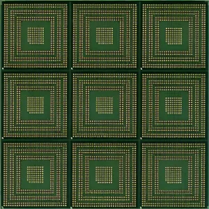
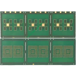
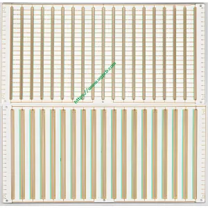
A BGA IC Substrate is a specialized type of ربط عالية الكثافة (مؤشر التنمية البشرية) ثنائي الفينيل متعدد الكلور designed explicitly for Ball Grid Array (بغا) التعبئة والتغليف. It is not a standard لوحة الدائرة but a precision multilayer interconnect structure. One side interfaces with the die via ultra-fine circuitry, while the opposite side connects to the main لوحة ثنائي الفينيل متعدد الكلور through an array of solder balls, fulfilling four key functions: الربط الكهربائي, نقل الإشارة, تبديد الحرارة, and physical support.
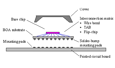
2. أساسيات التصميم & المبدأ التشغيلي
أساسيات التصميم:
-
Ultra-High Wiring Density: To accommodate increasing I/O counts, substrates require ultra-fine line design. UGPCB reliably achieves 30μm/30μm minimum line width/space, enabling efficient fan-out routing for high-pin-count chips.
-
Precise Registration & الاستقرار الأبعاد: Alignment between die and solder balls must be extremely accurate. Our core material, Mitsubishi Gas HF BT HL832NX-A-HS, offers a low CTE (معامل التمدد الحراري) واستقرار الأبعاد ممتازة, preventing warpage and misalignment caused by thermal stress.
-
Reliable Microvias: Layer-to-layer interconnection depends on laser-drilled blind vias. ملكنا 0.075mm laser drilling capability facilitates high-density vertical connections (على سبيل المثال, 1-2, 3-4 طبقات), ضمان سلامة الإشارة.
-
Optimized Signal & نزاهة السلطة: A carefully designed stack-up (على سبيل المثال, 1L-4L, 1L-2L, 3L-4L as per your specs) and plane allocation provide low-loss paths for high-speed signals and clean, stable power delivery to the chip.
المبدأ التشغيلي:
The die is attached to the substrate’s top surface (typically Layer 1) via wire bonding or flip-chip technology. Electrical signals from the chip are routed, redistributed (ردل), and transmitted through the substrate’s internal ultra-fine traces و فيا الدقيقة (laser/mechanical holes). They finally exit via the solder ball array on the bottom surface to connect to the larger ثنائي الفينيل متعدد الكلور (تجميع ثنائي الفينيل متعدد الكلور). It is essentially a miniaturized, chip-specific, الراقية لوحة الدوائر المطبوعة.
3. المواد الأساسية, بناء & الميزات الرئيسية
-
المواد الأساسية: Mitsubishi Gas HF BT HL832NX-A-HS high-performance laminate. Renowned for its ثابت عازل منخفض (DK), عامل تبديد منخفض (ص), مقاومة حرارية عالية (high Tg), and exceptional dimensional stability, it is the ideal choice for high-speed, high-frequency IC packaging substrates.
-
Key Structure: 4-layer build with stacked via design (1-2, 3-4 طبقة فيا أعمى) for greater routing density. The overall PCB thickness is 0.3mm, meeting thin-profile packaging requirements.
-
الانتهاء من السطح:****اينيبيك (النيكل غير الكهربائي البلاديوم الغمر الذهب, 2م”). This finish combines nickel’s barrier properties, palladium’s corrosion resistance, and gold’s superior solderability. It is the preferred choice for fine-pitch BGA solder ball مرفق, ضمان الموثوقية على المدى الطويل.
-
قناع اللحام & Opening: نحن نستخدم تايو PSR4000 AUS308 high-performance Liquid Photoimageable Solder Mask (إل بي إس إم), known for high resolution and reliability, perfectly defining openings for 0.1mm mechanical through-holes and pads.
4. تصنيف & التطبيقات الأولية
-
تصنيف: Primarily categorized by interconnection method: Wire Bonding Substrates و Flip Chip Substrates. The specifications provided (خطوط فائقة الدقة, اينيبيك) are particularly suited for Flip Chip and other advanced packaging applications.
-
التطبيقات الأولية:
-
وحدات المعالجة المركزية (CPU/GPU) التعبئة والتغليف
-
Mobile Device Application Processors (ا ف ب) & Baseband Chips
-
High-Speed Networking & Communication Chips (على سبيل المثال, FPGA, أسيك)
-
الذكاء الاصطناعي (منظمة العفو الدولية) & Machine Learning Accelerators
-
Advanced Memory Packaging (على سبيل المثال, إتش بي إم)
-
These applications represent the core of عالية الكثافة, high-performance PCBA تصميم.
-
5. UGPCB’s BGA IC Substrate Production Process & ضبط الجودة
ملكنا BGA circuit board manufacturing follows a stringent, high-standard flow:
Inner Layer Imaging → Laser Drilling / Mechanical Drilling → Hole Metallization (Copper Plating) → Outer Layer Imaging → Solder Mask Application (PSR4000) → ENEPIG Surface Finish → Electrical Testing → Final Inspection.
The entire process occurs in controlled cleanroom environments (Class 10K/1K), utilizing Automated Optical Inspection (الهيئة العربية للتصنيع), laser measurement systems, وأكثر, ensuring every BGA packaging PCB meets chip-level reliability standards.
6. Why Choose UGPCB for Your BGA IC Substrate?
-
Premium Material Assurance: Core laminates from top-tier suppliers like Mitsubishi Gas guarantee performance from the start.
-
قدرة العملية المتقدمة: 30/30μm line/space and 0.075mm laser microvias support the most cutting-edge chip packaging designs.
-
Ultra-Thin Core Expertise: Proven experience in high-yield, volume production of 0.3mm and thinner boards.
-
Comprehensive Surface Finish Options: We offer various high-end finishes including ENEPIG to meet different bonding/soldering needs.
-
خدمة وقفة واحدة: من مراجعة تصميم ثنائي الفينيل متعدد الكلور و نماذج أولية سريعة الدوران إلى حجم الإنتاج, we provide end-to-end PCBA substrate solutions for your new chip project.
خاتمة:
As we approach the physical limits of Moore’s Law, advanced packaging is key to continued electronics performance growth. Choosing a reliable BGA IC Substrate lays a solid foundation for your chip’s success. Whether you are involved in chip design, التعبئة والتغليف, اختبار, أو تصنيع ثنائي الفينيل متعدد الكلور, UGPCB هو شريكك الموثوق به.
اتصل بنا اليوم to discuss your BGA package substrate, اتش دي اي ثنائي الفينيل متعدد الكلور متطلبات, and request a quote. Let’s collaborate to enable the next generation of electronic innovation!