
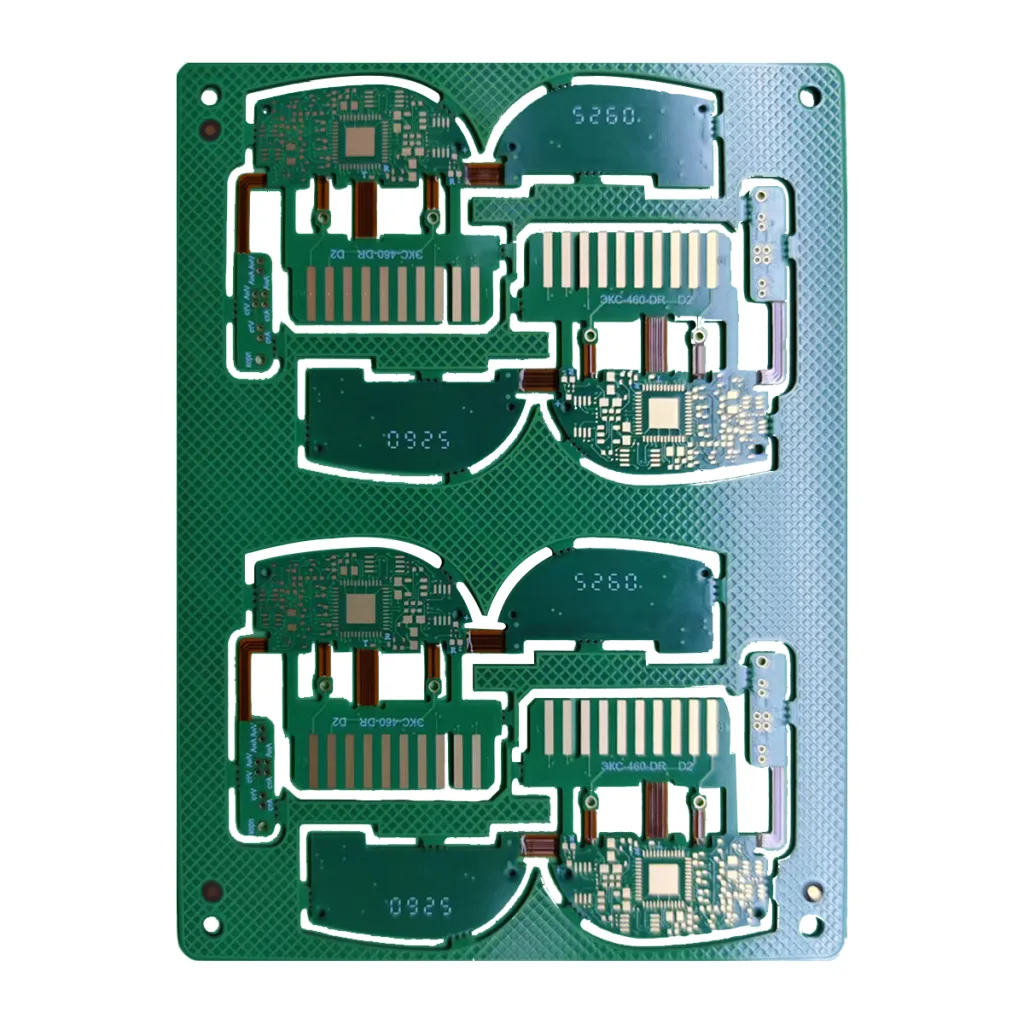
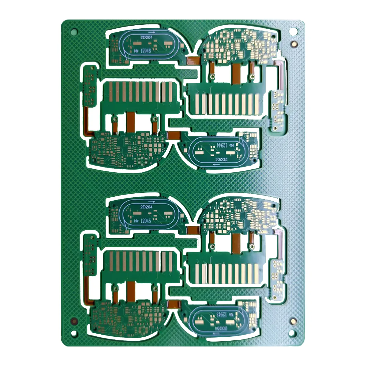
UGPCB’s 0.22mm Ultra-Thin 6-Layer HDI Rigid-Flex PCB Product Overview
In the pursuit of extreme device miniaturization and high reliability, traditional rigid لوحات الدوائر المطبوعة (مركبات ثنائي الفينيل متعدد الكلور) are often insufficient. UGPCB combines advanced ربط عالية الكثافة (مؤشر التنمية البشرية) و Rigid-Flex technologies to present our flagship product: ال 0.22mm Ultra-Thin 6-Layer HDI Rigid-Flex PCB. This board is a pinnacle of تصنيع ثنائي الفينيل متعدد الكلور و high-performance interconnect solution engineered for wearable technology, advanced medical instruments, الفضاء الجوي, and premium consumer electronics. It seamlessly merges the stable support of rigid boards with the dynamic bending capability of flexible circuits, enabling complex electrical connections within minimal space.
Product Definition & Scientific Classification
This is a high-layer-count PCB utilizing any-layer HDI و rigid-flex construction. It can be accurately classified per industry standards:
-
By Structure: ثنائي الفينيل متعدد الكلور جامد فليكس – Laminates rigid and flexible circuit layers into a single unit.
-
By Technology Level: Advanced HDI PCB – Employs laser drilling, filled vias, and microvias (<0.15مم) for superior routing density.
-
By Layer Count: 6-Layer Circuit Board (comprising both rigid and flexible layers).
-
By Material: Specialty High-Performance Material PCB – Core build-up uses Panasonic RF-777 composite.
Design Essentials & مبدأ العمل
Design Essentials: The key to a successful rigid-flex board design lies in the rigid-to-flex transition zone. Precise calculation of bend radius, stress relief, and routing in flex areas is critical to prevent cracking during dynamic flexing. في وقت واحد, HDI blind and buried via design must coordinate with the stack-up structure to optimize signal integrity (و) and power integrity (باي).
مبدأ العمل: ال هيكل ثنائي الفينيل متعدد الكلور integrates rigid sections (for component mounting and mechanical support) with flexible sections (for 3D interconnection and movement) عبر multilayer lamination. Electrical signals travel through laser-drilled microvias و via filling plating technologies inherent to لوحات HDI, achieving the shortest and most reliable paths between layers, which minimizes signal loss and crosstalk.
Core Materials & Superior Performance
-
Core Material: We utilize the industry-premium Panasonic RF-777 35/50 composite material. Renowned for its exceptional dimensional stability, superior high-frequency performance, and excellent heat resistance, it is the ideal choice for manufacturing high-reliability rigid-flex circuit boards.
-
الانتهاء من السطح: The board features a 2-micron Electroless Nickel Immersion Gold (يوافق) finish. This provides a flat surface, excellent solderability, and long-term oxidation resistance for PCB pads, making it perfect for mounting fine-pitch components like BGAs.
-
Key Performance Attributes:
-
Ultra-Thin 0.22mm Profile: Enables maximum compression of internal device space.
-
High Reliability: Undergoes rigorous PCB reliability testing, capable of withstanding millions of dynamic bend cycles.
-
Excellent Signal Transmission: HDI design and premium materials ensure low-loss transmission for high-speed signals.
-
High-Density Assembly: Provides an ideal platform for تجميع سمت, supporting miniaturized component layout.
-
بناء & الميزات الرئيسية
-
PCB Structure: A typical 6-layer construction involving 2-4 layers of rigid FR-4 laminated with polyimide flexible cores. ال stack-up is meticulously engineered to balance stiffness and flexibility.
-
Product Features:
-
3D Interconnection Freedom: Eliminates spatial constraints, enabling 3D assembly and reducing connectors and cables.
-
Lightweight & التصغير: The extreme thinness directly reduces product weight and size.
-
Enhanced System Reliability: Removes connection point failures, improving overall stability in vibrating or high-shock environments.
-
Simplified Assembly Process: As a custom تجميع ثنائي الفينيل متعدد الكلور, it streamlines final product assembly, lowering labor costs.
-
Precision Manufacturing Process
UGPCB adheres to international quality standards like IPC-6013 (for flexible circuits) و IPC-2221/2223. ملكنا PCB fabrication process is precise and rigorous:
-
حفر الليزر: Creates micron-level blind and buried vias in flexible and core layers.
-
Hole Metallization & تصفيح: Vias are made conductive through chemical deposition and plating, مع via filling for planarization.
-
Pattern Transfer & النقش: Forms the intricate circuit board traces.
-
طبقة محاذاة & التصفيح: Rigid layers, prepreg, and flexible layers are precisely aligned and bonded under high heat and pressure. This is the core step in rigid-flex PCB manufacturing.
-
التشطيب السطح: Application of the يوافق coating to protect pads and ensure solderability.
-
اختبار صارم: Includes flying probe testing, الفحص البصري الآلي (الهيئة العربية للتصنيع), and reliability testing to ensure every board’s quality.
Wide-Ranging Application Scenarios
هذا advanced PCB is the core skeleton for innovative products in:
-
Wearable Technology: Smartwatches, AR/VR glasses, health monitors, requiring comfort and constant flexing.
-
Advanced Medical Electronics: Endoscopic capsules, hearing aids, portable monitors, demanding high reliability and miniaturization.
-
الفضاء & الدفاع: Satellite components, UAV flight control systems, needing extreme environment endurance and low weight.
-
Precision Consumer Electronics: High-end smartphone camera modules, folding phone hinge areas, ultra-thin laptops.
-
صناعي & إلكترونيات السيارات: Compact sensors, robotic joint interconnection modules.

Contact a UGPCB PCB Technical Expert today for your 0.22mm Ultra-Thin HDI Rigid-Flex PCB solution! Make your product stand out in the competition for miniaturization and high performance.
 مع أعمى فيا")


 للوحدة")
")


