
Mini LED Packaging Substrate: The Core of Next‑Generation Display Technology
Mini LED packaging substrate is the critical carrier for micro‑pitch LED display technology. It not only provides physical support for LED chips but also ensures precise electrical signal transmission, efficient heat dissipation, and stable optical performance. As display technology rapidly advances toward pixel pitches below P1.0, the requirements for circuit precision, الإدارة الحرارية, and reliability of packaging substrates have become extremely stringent. Leveraging deep industry expertise, UGPCB introduces its Mini LED packaging substrate—engineered to meet the demand for ultimate performance in high‑end direct‑view displays and backlight modules.
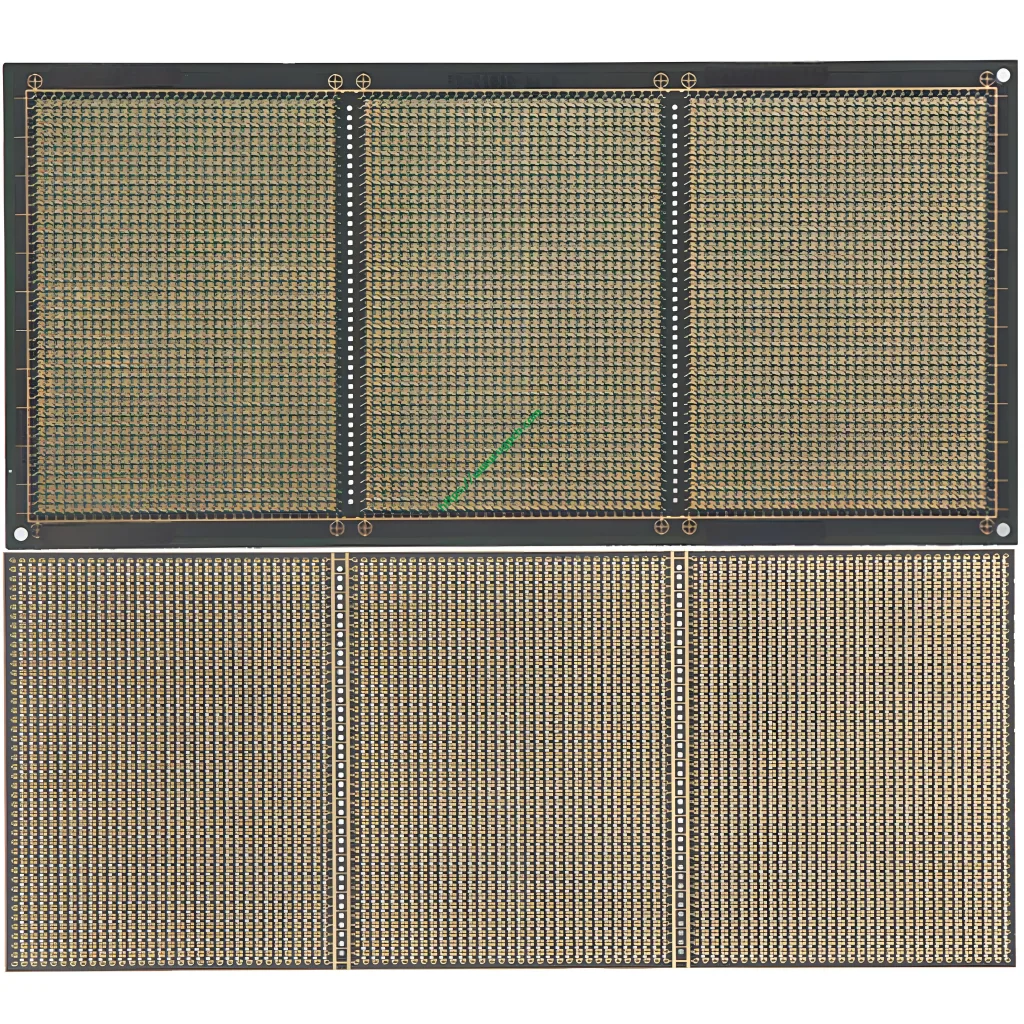
This substrate adopts a 4‑layer high‑density interconnect (مؤشر التنمية البشرية) بناء, with an overall thickness of only 0.5 مم and a unit size of 1.2 mm × 1.2 مم. Designed for advanced packaging processes such as chip‑level packaging (على سبيل المثال, MIP technology) and Chip‑on‑Board (COB), it addresses core challenges in micro‑pitch displays—including soldering reliability, الإدارة الحرارية, and signal integrity. It is the ideal foundation for seamless, high‑contrast, and highly reliable LED displays.
المواصفات الفنية الرئيسية & Interpretation
| Parameter Category | Specification | Technical Significance & Customer Value |
|---|---|---|
| بناء | 4‑layer, 0.5 mm total thickness | Enables separate routing for power, signal, and ground within a compact space, improving electrical stability and supporting slim module design. |
| Unit Size | 1.2 mm × 1.2 مم | Perfectly matches mainstream Mini LED chip dimensions, offering a standardized unit for display modules with P1.2 and finer pixel pitches. |
| Circuit Precision | دقيقة. line width: 30 ميكرومتر; دقيقة. space: 80 ميكرومتر | Meets ultra‑high‑density chip packaging requirements, enabling finer routing—essential for achieving micro‑pitch displays. |
| Processing Capability | دقيقة. hole diameter: 0.3 مم | Supports high‑density vertical interconnections, ensuring reliable electrical transmission between layers. |
| مادة & ينهي | مادة: دوسان (Korea); Solder mask: PSR‑4000 AUS308 (أبيض); الانتهاء من السطح: يوافق (الذهب الغمر بالنيكل غير الكهربائي) | Excellent high‑frequency and thermal performance; high‑reflectance solder mask boosts display contrast; ENIG provides superior solderability and oxidation resistance. |
Core Design Principles & Operating Mechanism
Successful Mini LED تصنيع ثنائي الفينيل متعدد الكلور starts with a superior substrate. UGPCB focuses on three critical design principles:
-
High‑Precision Patterning & تنسيق: ال 30 μm line width and 80 μm spacing represent a technological threshold. We employ modified Semi‑Additive Process (mSAP) و Laser Direct Imaging (LDI) to accurately etch insulation channels between tiny pads, effectively preventing micro‑short circuits or metal migration—foundational for high‑yield PCB production.
-
Exceptional Thermal Management: Mini LED chips exhibit high power density; heat accumulation accelerates luminous decay and reduces lifespan. Our high‑thermal‑conductivity substrate material, combined with optimized power‑layer design, creates an efficient heat‑conduction path, rapidly transferring heat from the chips to the system heatsink, ensuring long‑term display stability.
-
Reliable Solder & Packaging Interface: The ENIG surface finish offers excellent solderability, and its flat plating surface is ideal for mass chip transfer and eutectic bonding. This provides a solid foundation for subsequent SMT or die‑bonding processes, significantly improving overall تجميع PCBA yield and reliability.
Operating Principle: Through its internal high-precision copper traces, the substrate accurately distributes current and control signals from the driver IC to each Mini LED chip. معًا, it acts as a robust mechanical platform and thermal hub, supporting and protecting the fragile chips while dissipating operational heat—ensuring each pixel operates durably, stably, and efficiently.
التطبيقات الأولية & Classifications
Based on end‑use and technical approaches, UGPCB’s Mini LED packaging substrate serves two main fields:
-
Mini LED Direct‑View Display
The forefront of display technology, targeting seamless tiling for TVs and commercial large‑screen displays. Our substrate is ideal for:-
MIP Packaging: The substrate serves as a carrier unit for individual or multiple chips before being mounted onto the display driver board. This demands extremely high dimensional accuracy and pad consistency.
-
COB Packaging: LED chips are directly bonded onto the substrate before overall encapsulation. This requires outstanding heat resistance and adhesion to encapsulants—perfectly addressed by our material selection and surface treatment.
-
-
Mini LED Backlight Modules
Used primarily in high‑end TVs, gaming monitors, إلخ. هنا, the substrate carries thousands to tens of thousands of Mini LED chips as the backlight source, emphasizing uniform light distribution, wiring for local dimming zones, and reliability under prolonged high‑temperature operation. Our substrate ensures independent control of each backlight zone via high‑precision circuitry, enabling stunning picture quality with million‑to‑one contrast ratios.
Competitive Advantages
In a competitive market, UGPCB’s Mini LED packaging substrate builds a solid barrier through several core processes:
-
Finer Processing: Compared to traditional LED substrates or standard HDI PCBs, our 30 μm/80 μm line/space capability supports smaller chips and finer pixel pitches, enabling customers to achieve more detailed display quality.
-
More Robust Packaging Solution: Special dielectric filling and a process that embeds front‑side circuits address the industry challenge of ultra‑fine lines peeling or damaging during handling and use. This structure “locks” circuits firmly within the substrate, greatly enhancing mechanical strength and reliability.
-
Superior Thermal & Optical Performance: The high‑reflectance white solder mask (PSR‑4000 AUS308) maximizes light reflection from the chips, boosting screen brightness and contrast. Optimized layer‑up and material selection provide excellent thermal pathways, ensuring product longevity from the source.
Rigorous Production Process
We adopt advanced Substrate‑Like PCB (SLP) manufacturing flow to ensure every substrate meets design limits. Key steps include:
-
إعداد المواد & Patterning: Select coreless material; form precise front‑side circuits via lamination, exposure, تطوير, and plating.
-
Image suggestion: LDI or plating line in cleanroom.
ALT: Laser Direct Imaging (LDI) for high‑precision Mini LED substrate patterning – UGPCB SLP process
-
-
Buildup & حفر الليزر: Brown‑oxidation of circuits, followed by lamination of dielectric and copper foil. High‑precision laser drilling creates micro‑vias of 40–100 μm diameter.
-
Via Metallization & Backside Patterning: Electroless copper deposition makes blind vias conductive, followed by via‑filling plating. Back‑side circuit patterning is then completed.
-
Carrier Removal & قناع اللحام: Temporary carrier removal; fast‑etch technology embeds front‑side circuits into the dielectric and forms back‑side pads. High‑reflectance white solder mask is printed, followed by ENIG surface finish.
-
التفتيش النهائي & التعبئة والتغليف: After rigorous الفحص البصري الآلي (الهيئة العربية للتصنيع), electrical testing, إلخ., qualified products are vacuum‑packed in a Class‑1000 cleanroom, ready for delivery to customers for chip packaging and PCBA assembly.
Five Reasons to Choose UGPCB
-
Specialization & Focus: We are deeply experienced in high‑density PCBs, with thorough understanding of Mini LED technology evolution and pain points, offering full‑service solutions from design support to volume production.
-
القيادة التكنولوجية: Mastery of core processes such as 30 μm line width and 0.3 mm micro‑vias places us in the industry’s first tier, ready for future finer‑pitch products.
-
Proven Reliability: Raw materials sourced from reputable suppliers like Doosan Korea, combined with strict process control and full‑flow inspection, ensure product consistency and long‑term reliability.
-
Rapid Response: Our dedicated technical support team quickly addresses customer needs in design, process adaptation, and prototyping.
-
تحسين التكلفة: Through process innovation and scaled manufacturing, we deliver high performance while helping customers optimize overall BOM cost and enhance market competitiveness.
Equip Your Project with a Leading Display “Core” Foundation
Whether you are developing next‑generation Micro LED TVs, commercial tiled displays, or professional automotive display systems, a high‑performance, reliable packaging substrate is the starting point for success. UGPCB’s Mini LED packaging substrate solution combines extreme precision, outstanding reliability, and specialized service, aiming to be your most trusted partner.
Contact our technical sales team today for detailed technical documents, أ free تصميم ثنائي الفينيل متعدد الكلور review, or a customized sample plan. Let’s illuminate the future of display together.


