
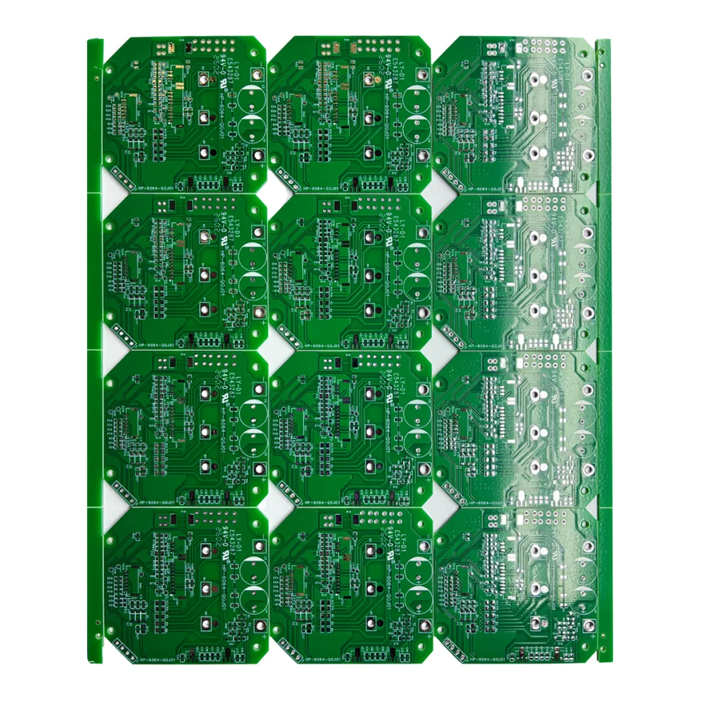
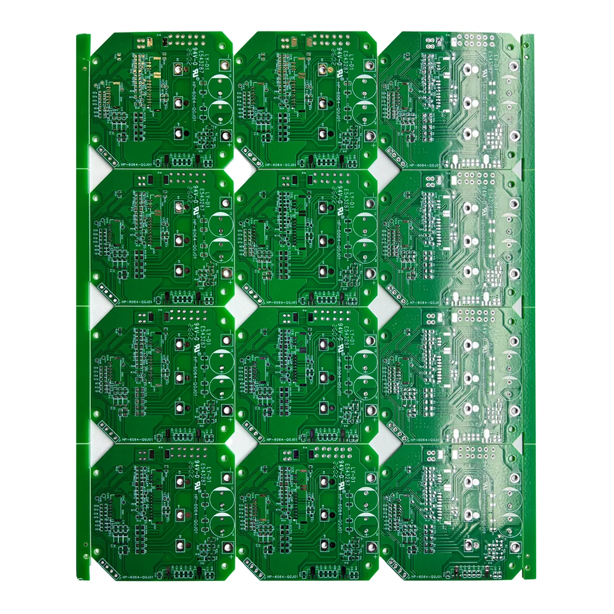
High-Performance FR-4 Double-Sided PCB Panoramica del prodotto & Definizione
Questo 2-Layer Rigid Circuito stampato (PCB) from UGPCB is a fundamental and widely used electronic interconnect solution. It features a standard 1.6mm board thickness, dimensions of 224.02mm x 189mm, and utilizes high-grade KB FR-4 laminato. This double-sided PCB serves as the essential “backbone” for electronic designs, providing reliable electrical connections and mechanical support for components. It is an ideal, cost-effective choice for a vast range of industrial control, elettronica di consumo, and power supply applications.
Considerazioni critiche sulla progettazione
Successful design of a double-sided PCB requires balancing electrical performance with manufacturability. Le considerazioni chiave includono:
-
Routing Strategy: Efficiently utilize both top and bottom layers for trace routing. Plated Through-Holes (PTHs or Vias) enable inter-layer connections. Careful planning of trace density is crucial to prevent signal integrity issues like crosstalk.
-
Hole & Pad Design: Specify appropriate drill sizes and pad diameters for all PCB vias and component leads to ensure mechanical strength and soldering reliability, aderendo a Standard IPC for annular ring.
-
Energia & Piani terrestri: While dedicated planes are absent, designers should widen power and ground traces or implement a gridded copper pour to reduce impedance and enhance stability—a key aspect of robust Progettazione di circuiti stampati.
-
Controllo delle regole di progettazione (Repubblica Democratica del Congo): Prior to fabrication, rigorously verify that all parameters (trace width/clearance, hole sizes) align with the manufacturer’s capabilities (as per this board’s specs) to guarantee PCB design for manufacturability (DFM).
Principio di lavoro & Struttura
The functionality of this double-layer circuit board stems from its layered structure:
-
Costruzione: The core consists of an FR-4 insulating dielectric layer, clad with copper foil (in genere 1 oz) on both sides. The unwanted copper is etched away during Fabbricazione di PCB, forming the desired circuit traces.
-
Electrical Interconnection: Circuits on the two layers are connected vertically via Plated Through-Holes (PTHS), created through mechanical drilling followed by electroless and electrolytic copper deposition.
-
Surface Protection: IL Livellamento per saldatura ad aria calda senza piombo (Sanguinare) finish applied to exposed copper pads prevents oxidation and ensures excellent solderability for component assembly.
Product Classification & Materiali
Per the provided specifications, this product is accurately classified as follows:
-
Per conteggio strati: PCB a doppia faccia O 2-PCB a livello.
-
Per rigidità del substrato: PCB rigido.
-
Per materiale di base: Scheda FR-4. Specificamente, FR-4 from the “KB” brand, an epoxy glass laminate known for superior electrical insulation, resistenza meccanica, and flame retardancy (UL94-V0).
-
Per finitura superficiale: Lead-Free HASL PCB.
-
By Application Complexity: Standard, General-Purpose Industrial-Grade PCB.
Prestazione & Caratteristiche chiave
Leveraging the specified materials and processes, this PCB delivers the following core performance benefits:
-
Reliable Mechanical & Prestazioni elettriche: IL KB FR-4 material offers stable dielectric constant and low dissipation factor for signal integrity. The 1.6mm standard thickness provides excellent resistance to bending and vibration.
-
Dependable Interconnections: IL Lead-Free HASL surface finish provides a flat, highly solderable coating compatible with both wave soldering and hand soldering processes.
-
Superior Thermal Stability: FR-4 substrate withstands standard soldering temperatures and offers a high continuous operating temperature, suitable for most Elettronica industriale environments.
-
High Cost-Effectiveness: Compared to multi-layer boards, double-sided PCBs offer significantly lower PCB fabrication cost and shorter lead times, representing an economical hardware solution.
-
Conformità ambientale: IL HASL senza piombo process complies with international directives such as RoHS.
Detailed Manufacturing Process
UGPCB aderisce a rigorosi, high-standard Processo di produzione dei PCB:
-
Engineering & CAM: Gerber file analysis, DFM check, and photoplot generation.
-
Panelization: Cutting the large FR-4 laminato rivestito di rame into production panels.
-
Perforazione: CNC drilling of component holes and PCB vias.
-
Hole Metallization: Desmear, chemical copper deposition, and electrolytic copper plating to form conductive Plated Through-Holes (PTHS).
-
Modellazione: Applicazione del fotoresist, esposizione, development to transfer the circuit image.
-
Incisione: Removing unwanted copper to form precise circuit traces.
-
Maschera di saldatura & Silkscreen: Applying LPI solder mask (typically green) and legend printing.
-
Finitura superficiale: Applying HASL senza piombo coating to exposed pads.
-
Routing & Test elettrici: Profiling to final board outline and performing Electrical Test (Sonda volante or Fixture Test).
-
Ispezione finale & Confezione: Comprehensive Ispezione ottica automatizzata (AOI), dimensional verification, and vacuum-sealed, moisture-proof packaging.
Applicazioni primarie & Casi d'uso
This specification of double-sided FR-4 PCB is widely deployed in reliable and cost-sensitive applicazioni:
-
Industrial Control Systems: PLC controllers, motor drive boards, sensor interface modules.
-
Power Supply Units: Switch-mode power supplies (SMPS), UPS systems, LED driver boards.
-
Elettronica di consumo: Appliance control boards (AC, washing machines), smart home controllers, apparecchiatura audio.
-
Elettronica automobilistica: Body control modules (BCM), lighting controllers, non-critical infotainment systems.
-
Telecommunications Equipment: Functional modules within routers, interruttori.
-
Test & Strumenti di misura: Data acquisition and display panels for equipment.

Why Choose UGPCB for Your Double-Sided PCB Needs?
Partnering with UGPCB guarantees:
-
Produzione di precisione: Strict adherence to 1.6mm thickness, 224.02x189mm dimensions, E Materiale FR-4 specifiche.
-
Process Excellence: Standardized Lead-Free HASL PCB production ensures batch-to-batch consistency and reliability.
-
Expert Technical Support: Our team provides comprehensive support, da Progettazione di circuiti stampati review to production consultation.
-
Fast Turnkey Delivery: We offer competitive lead times for standard double-layer PCB prototypes and production runs.
Ready to start your project? Contact UGPCB today for a competitive quote and expert support. Let us be your trusted Produttore di PCB and partner for success.


