

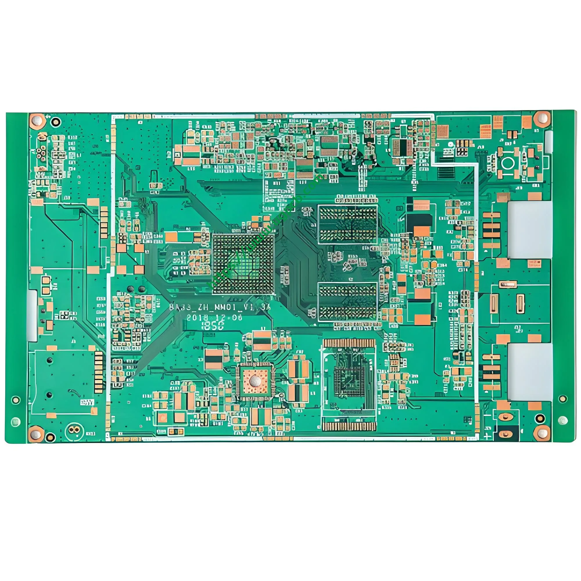
Panoramica del prodotto: Cos'è un circuito stampato PCB antiossidante OSP?
UNCircuito PCB antiossidante OSP usiConservanti di saldabilità organica (OSP) come la sua finitura superficiale in rame. Questo processo deposita una pellicola organica ultrasottile sulle superfici di rame nudo. La pellicola previene l'ossidazione durante lo stoccaggio e l'assemblaggio. Durante la saldatura, il flusso dissolve rapidamente la pellicola OSP. Ciò espone il rame pulito per giunti di saldatura affidabili.
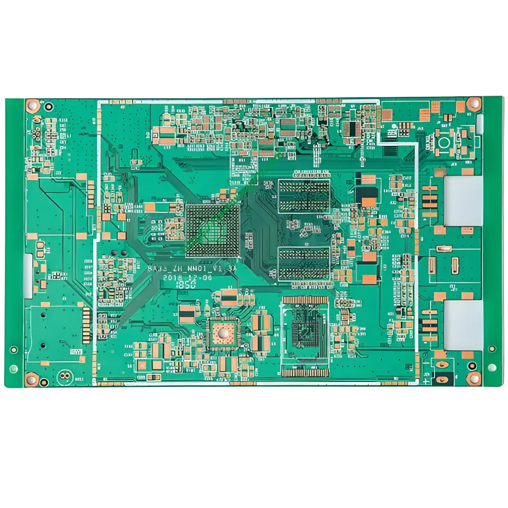
Utilizza il circuito stampato PCB antiossidante OSP di UGPCBLaminato epossidico in vetro FR-4 come materiale di base. Presenta 35μm (1 oz) lamina di rame, 1.6spessore tavola mm, e dimensioni di 68.36 × 34,6 mm. La dimensione minima del foro finito è 0,45 mm. La larghezza minima della traccia è 0,15 mm e la spaziatura minima è 0,20 mm. Il prodotto è pienamente conforme a IPC-6012E (qualificazione e prestazioni dei pannelli stampati rigidi) e IPC-4555 (prestazioni OSP ad alta temperatura) specifiche.
QuestoPCB OSP a doppia faccia serve l'elettronica di consumo, Attrezzatura di comunicazione, e controlli industriali. Funziona meglio dove la sensibilità ai costi e la planarità della superficie contano di più.
Classificazione scientifica dei prodotti
Basato sui sistemi internazionali di classificazione dei PCB, questo prodotto rientra in queste categorie:
| Dimensione Classificazione | Categoria |
|---|---|
| Materiale del substrato | PCB rigido in tessuto di vetro epossidico FR-4 |
| Numero di strati | A doppia faccia (circuiti a due strati) |
| Finitura superficiale | OSP (Conservanti di saldabilità organica) antiossidante |
| Punteggio di infiammabilità | UL 94 V-0 |
| Classe di prestazione IPC | Classe 2 (prodotti elettronici di servizio dedicato) |
| Spessore di lamina di rame | 1 oz (35μm) rame standard |
| Spessore della scheda | 1.6tavola rigida standard da mm |
| Tipo di foro | Foro passante compatibile con SMT |
Spiegazione dei principali parametri tecnici
Substrato: FR-4 Tessuto di vetro epossidico
FR-4 è il substrato rigido più comune nel PCB industria. “FR” significa ritardante di fiamma. “4” indica resina epossidica combinata con tessuto di vetro che incontraUL 94 V-0 standard di infiammabilità. UL 94 V-0 richiede che i campioni verticali si autoestinguano all'interno10 secondi dopo due applicazioni di fiamma da 10 secondi ciascuna. Nessuna goccia ardente può incendiare il cotone.

La temperatura di transizione del vetro (Tg) misura la resistenza al calore. La Tg standard dell'FR-4 varia da 130 a 140°C. L'FR-4 a Tg media raggiunge i 150–160°C. L'FR-4 ad alta Tg supera i 170°C. Questo prodotto utilizza lo standard FR-4 con Tg ≥ 130°C (Conforme a IPC-4101/21). Ciò soddisfa le esigenze di shock termico della saldatura a rifusione (temperature di picco 240–260°C).
Spessore di lamina di rame: 35μm (1 oz)
Lo spessore del rame determina la capacità di trasporto di corrente. Questo prodotto utilizza35μm lamina di rame, conosciuto come1 once di rame (1 oz/ft² ≈ 35μm). Secondo IPC-2221, 1 oz di rame a 10°C l'aumento di temperatura comporta circa:
- 0.15mm (6 mil) Larghezza della traccia: 0.5-0,7A
- 0.20mm (8 mil) Larghezza della traccia: 0.8-1,0 A
Lo spessore del rame di 35μm è lo standard più comune per i PCB a doppia faccia. Bilancia i costi, capacità attuale, e resa manifatturiera.
Dimensioni della scheda: 68.36 × 34,6 mm
Le misure della tavola finita68.36mm × 34,6 mm. Questa dimensione compatta si adatta ai moduli elettronici stretti. I PCB di piccole dimensioni richiedono una precisione più rigorosa: le tolleranze dimensionali in genere rimangono entro ±0,15 mm (Classe IPC-6012 2).
Dimensione minima del foro finito: 0.45mm
0.45mm è il foro passante minimo placcato (PTH) diametro. Questa dimensione del foro è uno standard nel settore. Garantisce una placcatura affidabile (proporzioni approssimative 3.6:1 con spessore del pannello di 1,6 mm). La dimensione del foro è adatta alla maggior parte dei componenti DIP e ai modelli di pad SMT standard.
Spessore del PCB: 1.6mm
1.6mm è lo spessore della scheda più comune nella produzione di PCB. Fornisce un'eccellente resistenza meccanica e rigidità alla flessione. Si adatta perfettamente ai connettori e alle prese standard.
Larghezza e spaziatura: 0.15mm / 0.20mm
Questo prodotto offrelarghezza minima della traccia di 0,15 mm (Di 6 mil) Edistanza minima di 0,20 mm (Di 8 mil). Secondo la classificazione IPC, in cui rientrano queste dimensioniClasse 2 (prodotti elettronici di servizio dedicato). Questa precisione soddisfa la maggior parte dei progetti PCB a media densità, comprese le schede di controllo MCU, moduli di gestione dell'energia, e schede convertitori di interfaccia.
Come funziona il processo antiossidante OSP
Il processo OSP fa crescere una pellicola organica ultrasottile su rame nudo e pulitoadsorbimento chimico. Il film OSP è composto principalmente dacomposti alchil benzimidazolici (a base di azoli). Lo spessore del film varia tipicamente da0.2–0,5μm.
Meccanismo di protezione
Il film OSP protegge le superfici in rame attraverso tre meccanismi:
- Barriera fisica – Il film organico forma uno strato molecolare denso. Impedisce all'ossigeno e all'umidità di entrare in contatto con la superficie del rame.
- Adsorbimento chimico – I gruppi attivi nelle molecole OSP si legano chimicamente con gli atomi di rame. Questo crea una forte adesione.
- Protezione selettiva – La pellicola OSP copre solo le aree in rame. Non influisce sulla maschera di saldatura o su altre regioni non metalliche.
Comportamento durante la saldatura
Durante il riflusso SMT, raggiungono le temperature190–230°C. I principi attivi del fondente si decompongono e dissolvono la pellicola OSP. Questo espone il rame pulito sottostante. La saldatura contatta direttamente il rame nudo e le formecomposti intermetallici (IMC). Ciò crea collegamenti elettrici affidabili. Il film dell'OSPsi decompone completamente senza residui dopo la saldatura.
Caratteristiche chiave delle prestazioni
Basato sui metodi di prova IPC-TM-650:
| Caratteristica | Valore tipico / Requisito | Norma di riferimento |
|---|---|---|
| Spessore della pellicola OSP | 0.2–0,5μm | IPC-4555 |
| Angolo di bagnatura della saldatura | ≤30° (Dopo 1 Reflaow) | IPC-TM-650 2.4.1 |
| Rapporto di diffusione della saldatura | ≥80% | IPC-TM-650 2.4.1 |
| Protezione dall'ossidazione (ambientale) | ≥6 mesi | IPC-4555 |
| Modifica della resistenza di contatto | ≤10% (Dopo 6 mesi di conservazione) | IPC-TM-650 |
Processo di produzione di PCB antiossidanti OSP
La produzione di PCB antiossidanti OSP segue rigorosi controlli di processo. Ogni passaggio influisce sulla qualità e sull'affidabilità finale.
Processi front-end (Preparazione del substrato & Pattern del circuito)
- Taglio del materiale – Tagliare a misura il laminato rivestito in rame FR-4
- Perforazione – Foratura CNC con dimensione minima del foro di 0,45 mm
- Rame chimico / Galvanotecnica – Metallizzare le pareti dei fori per la connessione strato-strato
- Trasferimento del modello di circuito – Pellicola secca / esposizione e sviluppo di film umido
- Incisione – Rimuovere il rame indesiderato per creare una traccia di 0,15 mm / 0.20Circuiti con spaziatura mm
- Stampa della maschera di saldatura – Applicare inchiostro per maschera di saldatura verde o di altro colore
- Pre-pulizia – Rimuovere ossidi e contaminanti prima della finitura superficiale
Processo di rivestimento OSP (Processo fondamentale)
Il tipico flusso di rivestimento OSP:
Sgrassaggio → Doppio risciacquo con acqua → Micro-incisione → Doppio risciacquo con acqua → Decapaggio acido → Risciacquo con acqua DI → Formazione di pellicola OSP → Asciugatura all'aria → Risciacquo con acqua DI → Asciugatura finale
- Microincisione – Rimuove gli ossidi di rame e crea una superficie uniforme microscopicamente ruvida. Ciò promuove la crescita del film OSP.
- Formazione del film OSP – Immergere il PCB nella chimica OSP (alchil benzimidazolo, acidi organici, cloruro di rame, e acqua deionizzata). Il film cresce attraverso l'adsorbimento chimico sulle superfici di rame.
- Controllo dello spessore del film – Il controllo preciso è fondamentale. Troppo sottile significa scarsa resistenza al calore. Uno spessore eccessivo ostacola l'azione del flusso e il flusso della saldatura.
Processi back-end
- Instradamento – Instradamento CNC alle dimensioni finali
- Test elettrici – Test di sonde volanti o dispositivi
- Ispezione finale – Ispezione visiva e campionamento dello spessore del film
- Confezionamento sottovuoto – Imballaggio resistente all’umidità e all’ossidazione
Caratteristiche del prodotto e vantaggi principali
Eccellente planarità superficiale
Il film OSP è solo0.2–0,5μm spesso. Si forma per adsorbimento chimico con spessore uniforme e superficie liscia. Ciò preserva la planarità originale della lamina di rame. È l'ideale perSMT a passo fine componenti (come QFP con passo 0,4 mm e inferiore, Pacchetti QFN).
Saldabilità superiore
La pellicola OSP si dissolve rapidamente nel flusso durante il riflusso. Ciò espone il rame fresco per una formazione IMC affidabile. Il processo OSP supporta entrambiforo passante (Tht) Emontaggio superficiale (SMT) saldatura.
Conveniente
OSP non utilizza metalli preziosi (oro, argento, palladio). I costi dei materiali e della lavorazione sono inferiori a quelli dell'ENIG, argento ad immersione, o stagno per immersione. Per la produzione in grandi volumi come l'elettronica di consumo, OSP offre un'eccezionale competitività in termini di costi.
Conforme all'ambiente
L'OSP utilizza composti organici. Non contiene piombo, mercurio, cadmio, o cromo esavalente. Soddisfa pienamenteRoHS 2.0 Requisiti. Anche i costi e la complessità del trattamento dei rifiuti sono inferiori rispetto ai processi di finitura dei metalli.
Breve tempo di elaborazione
Il rivestimento OSP è semplice e veloce. Non necessita di complesse apparecchiature di placcatura o di lunghi tempi di deposizione. Rispetto all'ENIG (che richiede ore), OSP completa la finitura superficiale in30–60 minuti per lotto. Ciò riduce notevolmente i tempi di consegna.
Linee guida di progettazione e considerazioni importanti
Progettazione per la produzione (DFM) Regole
In base alle capacità di processo di questo prodotto:
| Parametro di progettazione | Capacità del prodotto | Valore di progettazione consigliato |
|---|---|---|
| Larghezza minima di traccia | 0.15mm | ≥0,15 mm (tracce di segnale) |
| Spaziatura minima | 0.20mm | ≥0,20 mm |
| Dimensione minima del foro | 0.45mm | ≥0,45 mm |
| Spessore della scheda | 1.6mm | 1.6mm (standard) |
Limitazioni e mitigazioni del processo OSP
L'OSP offre molti vantaggi ma presenta limitazioni intrinseche:
- Durata di conservazione limitata – La pellicola OSP protegge6 mesi in condizioni ambientali. Per la migliore saldabilità, assemblaggio SMT completo all'interno 3 mesi.
- Sensibilità all'umidità – Le pellicole OSP si degradano alle alte temperature, ambienti ad alta umidità. Conserva le tavole presso20–25°C con umidità relativa del 40–60%..
- Cicli di riflusso limitati – Resistenze OSP standard1–2 shock termici di riflusso. Riflussi multipli richiedono OSP ad alta temperatura (Conforme allo standard IPC-4555).
- Sfide di test elettrici – La pellicola OSP è isolante. Influisce sull'affidabilità del contatto di test elettrico. I punti di prova necessitano della stampa della pasta saldante per rimuovere lo strato OSP.
Raccomandazioni per la conservazione e la manipolazione
- Confezione sottovuoto con essiccante e schede indicatrici di umidità
- Ambiente di archiviazione: temperatura ≤30°C, umidità relativa ≤60%
- Saldatura completa all'interno48 ore dell'apertura del pacco
- Indossare guanti antistatici durante la manipolazione. Evitare il contatto a mani nude con le superfici della tavola.
Scenari di applicazione tipici
I circuiti stampati PCB antiossidanti OSP servono molti settori grazie alla lorovantaggio di costo, planarità della superficie, ed eccellente saldabilità:
Elettronica di consumo
- Schede madri per smartphone e PCB per tablet
- Schede madri e schede grafiche per computer
- Schede di controllo degli elettrodomestici
- Circuiti stampati per dispositivi indossabili
Attrezzatura di comunicazione
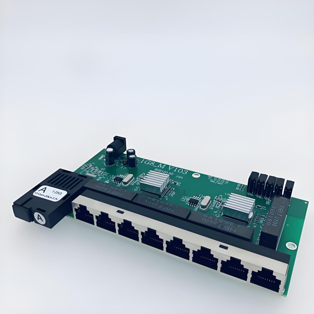
- Router e switch PCB
- Moduli di comunicazione e dispositivi IoT
- Bluetooth / Schede porta moduli Wi-Fi
Controlli industriali
- Controllori logici programmabili PLC
- Moduli di gestione dell'energia
- Schede elettroniche di strumentazione
- Schede di controllo dell'azionamento del motore
Elettronica automobilistica (Non critico per la sicurezza)
- Sistemi di infotainment di bordo
- Moduli di controllo del corpo
- Schede di interfaccia sensori
Garanzia di qualità e conformità agli standard
Standard applicabili
Il prodotto PCB antiossidante OSP di UGPCB segue rigorosamente questi standard internazionali:
| Standard | Titolo | Ambito |
|---|---|---|
| IPC-4555 | Specifiche prestazionali per conservanti organici di saldabilità ad alta temperatura (OSP) per schede stampate | Requisiti e test del processo OSP |
| IPC-6012E | Specifiche di qualificazione e prestazione per circuiti stampati rigidi | Qualità e prestazioni della tavola finita |
| IPC-4101/21 | Specifiche per laminato epossidico rinforzato con vetro | Requisiti tecnici del substrato FR-4 |
| IPC-TM-650 | Manuale dei metodi di prova | Vari metodi di test delle prestazioni |
| UL 94 V-0 | Infiammabilità delle materie plastiche | Sicurezza ignifuga del substrato |
| RoHS 2.0 | Limitazione delle sostanze pericolose | Conformità ambientale |
Indicatori chiave di qualità
Secondo i requisiti IPC, le metriche chiave della qualità includono:
- Spessore della pellicola OSP: 0.2–0,5μm, tolleranza di uniformità ≤ ±0,1μm
- Adesione: ≥4B (IPC-TM-650 2.4.29 prova trasversale)
- Rapporto di diffusione della saldatura: ≥80% (IPC-TM-650 2.4.1)
- Periodo di protezione dall'ossidazione: ≥6 mesi (condizioni ambientali)
- Punteggio di infiammabilità: UL 94 V-0
Perché scegliere UGPCB per PCB antiossidanti OSP?
Capacità di produzione di precisione
- 0.15larghezza minima della traccia mm / 0.20spaziatura minima mm
- 0.45dimensione minima del foro finito mm
- 1.6Spessore pannello standard mm con eccellente compatibilità
Controllo affidabile del processo OSP
- Aderenza rigorosa allo standard IPC-4555 per spessore e qualità del film
- Tracciabilità completa durante tutto il processo di produzione
- Test di saldabilità e campionamento dello spessore del film per ogni lotto
Consegna veloce
- Tempi di consegna standard: 7–10 giorni lavorativi
- Supporta sia il campionamento dei prototipi che la produzione in serie
Supporto tecnico completo
- Revisione gratuita del progetto DFM
- Team di ingegneri professionisti per la guida alla selezione del prodotto
Ottieni un preventivo oggi stesso
UGPCB offre soluzioni di circuiti stampati PCB antiossidanti OSP di alto valore. Se ne hai bisognocampionamento del prototipo Oproduzione in volume, forniamo supporto tecnico professionale e prezzi competitivi.
📞 Come ottenere un preventivo:
- Invia i tuoi file Gerber e l'elenco BOM
- Il nostro team di ingegneri risponde con una soluzione personalizzata e un preventivo all'interno24 ore
- Controllo DFM gratuito per garantire che il tuo progetto venga superato al primo tentativo
Dichiarazione sull'origine dei dati: I dati tecnici e i requisiti standard citati in questo documento derivano principalmente da IPC (Associazione che collega le industrie elettroniche) standard tra cui IPC-4555 “Specifiche prestazionali per conservanti organici di saldabilità ad alta temperatura (OSP) per schede stampate,” IPC-6012E “Specifiche di qualificazione e prestazione per circuiti stampati rigidi,” IPC-4101/21 “Specifiche per laminato epossidico rinforzato con vetro,” IPC-TM-650 “Manuale dei metodi di prova,” e UL 94 “Norma per prove di infiammabilità di materie plastiche per parti di dispositivi ed apparecchi.” Alcuni parametri di processo fanno riferimento a dati tecnici disponibili al pubblico dei principali produttori di PCB. Tutti i dati sono stati verificati per l'accuratezza.













