
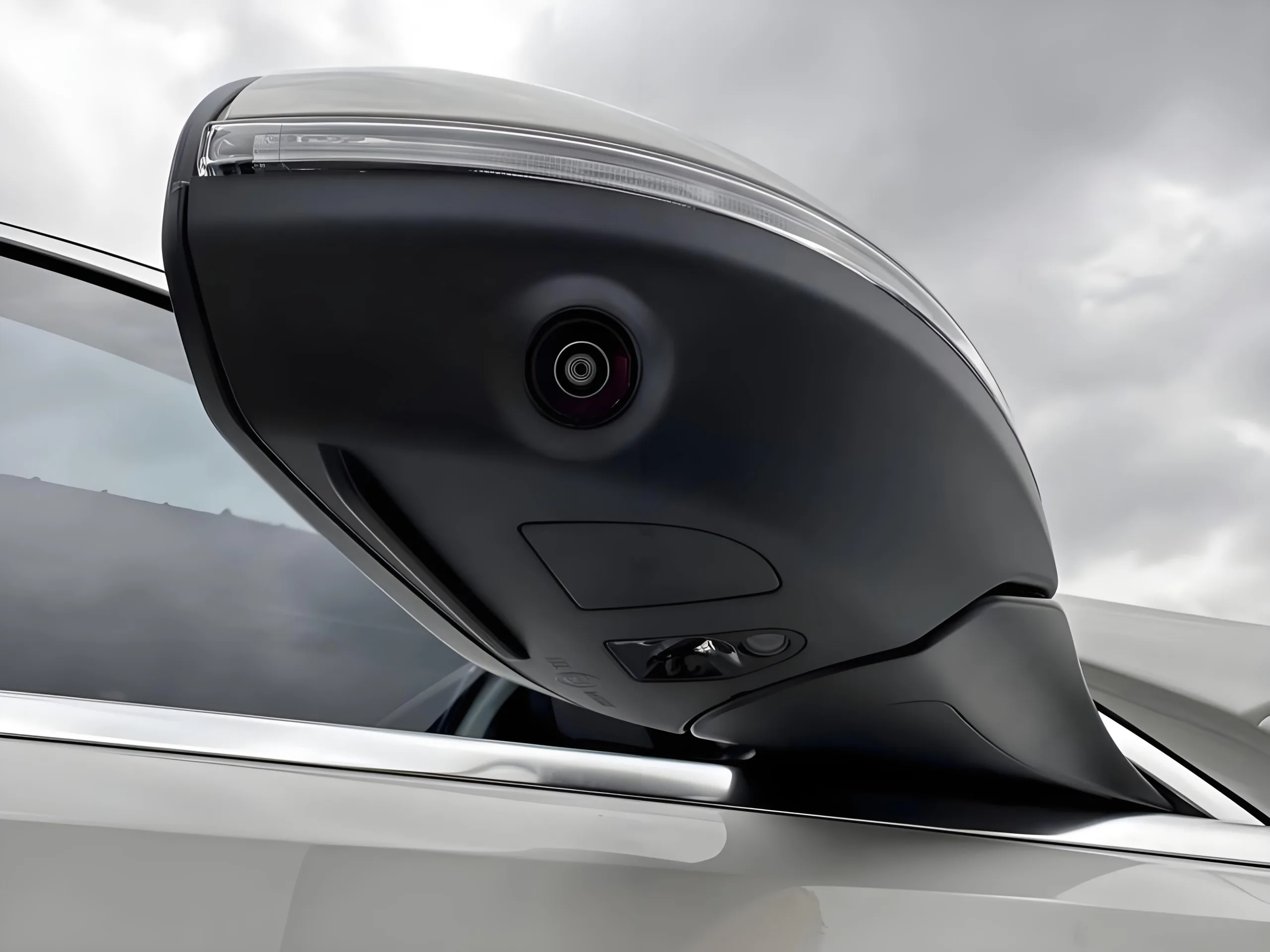
最先端のイノベーションを実現するために設計
スマートフォンのベゼルレスディスプレイとマルチレンズカメラシステムへの進化, 医療用内視鏡検査における小型化の需要と相まって, 普遍的な課題を提示する: 内部スペースを 1 ミリメートル単位で節約することで、大幅な設計上のメリットが得られます。. 従来のリジッド プリント基板 曲がらない, 一方、フレキシブル回路 (FPCS) コンポーネントが密集した領域では適切なサポートが不足していることがよくあります.
UGPCB その先進性を紹介します リジッドフレックスカメラモジュールPCB, FR-4 の機械的安定性とポリイミドの動的柔軟性を巧みに組み合わせたソリューション (PI). この革新的な相互接続により、コネクタやハーネスが不要になります, 直接提供する, 信頼性のある, コンパクトカメラシステム用のスペース効率の高いリンク.

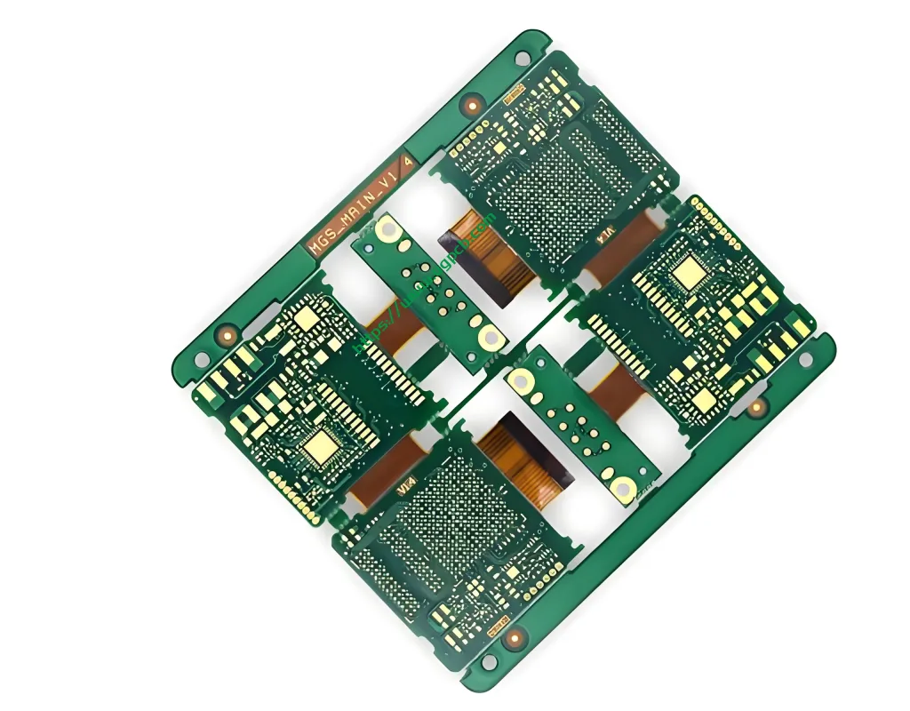
1. 製品の概要: リジッドフレックスカメラモジュールPCBの定義
あ リジッドフレックスPCB リジッド基板とフレキシブルケーブルをコネクタで接続するだけの単純な組み立てではありません. モノリシックです, 薄いものを重ね合わせた分離不可能な構造, 高度な真空ラミネートプロセスによる堅牢な FR-4 エポキシガラス強化コアを備えたフレキシブルなポリイミド基板 .
UGPCB の製品は、特に次の用途に向けて設計されています。 カメラモジュール. 特徴は、 2-レイヤーリジッド + 2-柔軟なレイヤー 工事. この設計は、従来のセットアップに見られるかさばるコネクタやケーブルを置き換えます。, CMOSイメージセンサーとメインアプリケーションプロセッサ間の信号経路を大幅に短縮.
2. 設計原則: 剛性と柔軟性のバランスをとる技術
このタイプの PCB を設計するには、電気的性能と機械的耐久性のバランスをとるための正確な 3D 計画が必要です。. UGPCB のエンジニアリングは、いくつかの重要な側面に重点を置いています:
-
スタックアップアーキテクチャ: デザインは左右対称の構造を採用しています。 剛性部の厚さは0.4mm そしてa フレキシブル部の厚さはわずか0.15mm. この正確な制御により、曲げの際に, フレキシブル領域の中性軸は銅導体と一致します, 応力を大幅に軽減し、痕跡の破壊を防止します.
-
移行ゾーン管理: 硬い領域と柔軟な領域の間の境界面は、製品の最も重要なゾーンです. UGPCB は 接着剤の流れを制御する技術 繰り返しの屈曲サイクル中の層間剥離や応力集中を防止するためのプラッギングを介して.
-
信号の完全性: 最新のイメージセンサーからの高速データを処理するため, 厳密なインピーダンス制御を遵守した設計, によって促進される 最小トレース/スペース 3mil/3mil. これによりクリーンな信号伝送が保証されます, 画質を劣化させる可能性のあるノイズや干渉がないこと.
3. 材料 & パフォーマンス: 品質の基盤の上に構築
この PCB の卓越したパフォーマンスは、厳選された高級素材から生まれています。:
-
硬質層材料: 高級品 FR-4 必要な機械的強度を提供します. CMOSセンサーの実装において絶対的な平面度を保証します。, カメラモジュールの正確な焦点面を維持するための交渉の余地のない要件.
-
フレキシブル層の材質: ポリイミド (PI) フィルムは柔軟な層の業界標準です . PI は優れた耐熱性を提供します (鉛フリーリフロープロファイルに耐える), 静的曲げ用途と動的曲げ用途の両方に優れた曲げ耐久性, 優れた化学的安定性.
-
表面仕上げ: PCB の特徴は、 エレクトロレスニッケルエレクトロレスパラジウムイマージョンゴールド (エネピック) 仕上げる. この高度な表面処理により、ニッケルの層が堆積されます。, パラジウム, そして金 . 完全に平らな表面を提供します, 小型部品に対する優れたはんだ付け性, アルミニウムまたは金のワイヤボンディングに最適です, センサーのパッケージングでしばしば必要となる .
4. 主な仕様
次のパラメータは、UGPCB の高精度機能を示しています。, 小型化された製造:
-
モデル: リジッドフレックスカメラモジュールPCB
-
素材の組み合わせ: FR-4 (剛性) + PI (フレックス)
-
レイヤー構成: 剛性 2 レイヤー / フレックス 2 レイヤー
-
はんだマスク色: 緑 / 白 (オプション)
-
仕上がり厚さ: 硬質部 0.4mm / フレックスエリア 0.15mm
-
銅の重量: 1 オンス (約. 35μm)
-
最小線幅/スペース: 3ミル / 3ミル
-
表面処理: エネピック (ニパダウ)
-
主な用途: カメラモジュールPCB (スマートフォン用, 自動車, 医学, ドローン)
5. それがどのように機能するか: 構造と機能
構造的に, この PCB は次のように視覚化できます。 “硬い島” 上に浮かんでいる “柔軟な海。”
-
リジッドゾーン: 厚いほど (0.4mm) FR-4 エリアは、イメージ センサーと受動部品の取り付けプラットフォームとして機能します。. この剛性により、オートフォーカスや光学式手ぶれ補正時の安定性が保証されます。, センサーを接続するはんだ接合部は機械的ストレスを受けません.
-
フレキシブルゾーン: 超薄型 (0.15mm) PI ベースの領域はリボン ケーブルとして機能します, 高速画像データをリジッドアイランドからメインロジックボードにルーティングします。. 薄い形状なので、しっかりと Z 字型または U 字型に折りたたむことができます。, スマートフォン内の限られたスペースにぴったりフィット, ドローン, または内視鏡カメラ.
-
動作原理: カメラのセンサーに光が当たると, 生成された電気信号は、フレキシブルゾーン内の精密にエッチングされた銅配線を通って伝わります。. これらの信号の完全性は、インピーダンス制御された設計によって維持されます。, 最終画像が鮮明でアーティファクトがないことを保証します.
6. 製造工程: 精度の旅
UGPCB は業界をリードするプロセスに従っています, IPC標準に準拠, 各リジッドフレックス PCB が最高の信頼性基準を満たしていることを確認します。 :
-
材料の準備 & クリーニング: FR-4およびPI基材を所定のサイズにカット. PI 材料は表面エネルギーを高めるためにプラズマ処理を受けています。, ラミネート時の強力な接着力を確保.
-
内層イメージング: フォトリソグラフィーの使用, 罰金 3ミル 回路は硬い層と柔軟な層の両方にエッチングされます. 自動光学検査 (あおい) オープンやショートなどの欠陥がないことを確認します .
-
ラミネート加工 & 真空接合: 準備した内層にボンディングシートを重ねます (プリプレグ) 真空環境下で高温高圧下でラミネート加工します。. このプロセスにより、剛性セクションと柔軟なセクションが単一のセクションに融合されます。, 不要な接着剤のにじみのない分離不可能なユニット .
-
掘削 & メッキ: 機械式と UVレーザー穴あけ加工 層相互接続用のマイクロビアを作成する. これらの穴は無電解銅めっきによって導電性にされ、電気めっき銅で補強されます。.
-
外層 & 表面仕上げ: 外部回路層が形成される, 続いて、 エネピック 表面仕上げ.
-
カバーレイの用途 & プロファイリング: 保護ポリイミドカバーレイが適用されます. レーザー切断 その後、正確に使用されます “開ける” パッドの上にカバーレイを重ね、最終的なボード形状のプロファイルを作成します。, デリケートなフレックスエリアに機械的ストレスをゼロにします。 .
7. 科学的分類
業界標準に従って, この製品は次のように分類されます:
-
構造によって: 多層リジッドフレックスプリント基板 (具体的には2R+2F構造).
-
アプリケーションによって: 光電子モジュール PCB (カメラモジュール).
-
テクノロジーによって: HDI リジッドフレックス PCB, 微細な3milのトレース幅とマイクロビアの要件により.
8. アプリケーション: スマートフォンを超えて
カメラモジュールに最適化されながらも, この PCB の特性により、要求の厳しいさまざまなアプリケーションに最適です。:
-
家電: 主力スマートフォンのマルチカメラモジュール, 折りたたみ式デバイスのカメラ, 超スリムなラップトップのウェブカメラ.
-
カーエレクトロニクス: 360-度サラウンドビューカメラとドライバーモニタリングシステム (DMS). これらの環境では、極端な振動や温度変動下での信頼性が求められます。 (-40°C ~ +85°C), リジッドフレックスボードによりコネクタ故障のリスクが排除される.
-
医療機器: 小型内視鏡とイメージングプローブ. 極度の薄さと高い信頼性の組み合わせにより、高解像度ビデオを送信しながら小さなキャビティへの挿入が可能になります.
9. カメラモジュールのニーズにUGPCBと提携する理由?
-
スペースのロックを解除する: 0.4mm のリジッドゾーンと 0.15mm のフレキシブルゾーンの組み合わせにより、 60% 従来と比較してスペースの拡大 “基板からケーブルまで” 相互接続ソリューション.
-
信頼性の向上: コネクタやはんだ接合をなくすことで、, 高振動環境での故障率を最大で削減できます。 70%.
-
信号忠実度を保証: 高精度 3mil/3mil ラインにより、MIPI などの高速インターフェースの安定した伝送チャネルを確保, センサーからプロセッサまで画像の完全性を維持.
見積もりを取得して次世代製品を強化してください
UGPCB は単なるメーカーではありません; 私たちはイノベーションのパートナーです. 主力スマートフォンを開発している場合でも、最先端の医療画像デバイスを開発している場合でも, 私たちの リジッドフレックスカメラモジュールPCB スペースに対する最も厳しい要件を満たすように設計されています, 重さ, と信頼性.
ガーバー ファイルまたはデザインに関するお問い合わせを次の宛先に送信してください。 [sales@ugpcb.com] . 当社のエンジニアリングチームがプロフェッショナルな DFM を提供します (製造可能性のための設計) 分析と競争力のあるボリューム見積もり 24 時間. 信頼できる精度を得るには UGPCB を選択してください.


普段コメントはしませんが、この特別な投稿には敬意を表したいと思います : D.