
Nos campos de design de PCB de alta velocidade e circuitos de RF, A continuidade da impedância é crucial para a integridade do sinal. A incompatibilidade de impedância característica pode levar à reflexão do sinal, toque, e distorção, afetando severamente o desempenho do sistema. Este artigo investiga as causas da descontinuidade de impedância e fornece soluções comprovadas pela indústria para ajudar os engenheiros a otimizar Designs de PCB.
Compreendendo a impedância característica e sua importância
Impedância Característica é um conceito central em PCB de alta frequência transmissão de sinal. De acordo com o padrão IPC-2141A, à medida que um sinal se propaga ao longo de uma linha de transmissão, um campo elétrico é formado entre a linha de sinal e o plano de referência, criando uma corrente instantânea. Se a linha de transmissão for uniforme, uma resistência equivalente é formada, definido como a relação entre tensão e corrente (Z=V/I). Esta é a impedância característica.
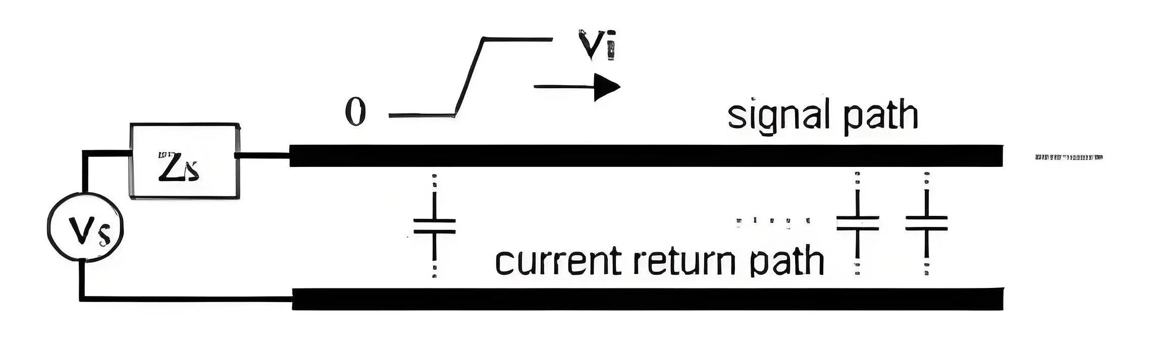
Quando a impedância característica muda ao longo do caminho de transmissão, a reflexão do sinal ocorre no ponto de descontinuidade. Esta reflexão pode causar distorção do sinal, erros de tempo, e interferência eletromagnética (EMI) problemas. De acordo com pesquisa do IEEE, um desvio de impedância superior 10% pode degradar gravemente a integridade do sinal.
Fatores-chave que afetam a impedância característica
A impedância característica é influenciada principalmente por quatro parâmetros: Constante dielétrica (Dk), espessura do substrato (h), largura do traço (c), e espessura do cobre (t). A fórmula de impedância característica para uma linha de microfita pode ser aproximada como:
Z0 = (87 / √(εr + 1.41)) * ln(5.98h / (0.8c + t))
Onde εr é a constante dielétrica relativa do substrato. Esta fórmula, derivado do padrão IPC-2141, é adequado para cálculos preliminares, mas ferramentas profissionais de cálculo de impedância devem ser usadas para projetos reais.
Cinco problemas comuns de descontinuidade de impedância e suas soluções
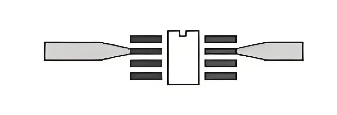
1. Mudanças repentinas na largura do traço e design de linha cônica
Muitos componentes de RF têm pacotes pequenos, com larguras de pad SMD potencialmente tão pequenas quanto 12 milésimos, enquanto os traços de sinal de RF geralmente exigem larguras acima 50 milésimos. Esta diferença de tamanho causa descontinuidade significativa de impedância.
-
Solução: Use linhas cônicas para transições; evite mudanças abruptas de largura. A conicidade deve ser suave, e seu comprimento não deve ser excessivo. De acordo com as diretrizes IPC-2221, a inclinação cônica deve ser mantida entre 1:3 e 1:5 para garantir uma mudança gradual de impedância.
2. Otimização de Cantos de Linhas de Transmissão
Curvas em ângulo reto em traços de sinal de RF aumentam a largura efetiva do traço, levando à descontinuidade da impedância e reflexão do sinal.
Solução: Aplicar mitras ou cantos arredondados. O raio de um canto arredondado deve satisfazer R > 3C (onde W é a largura do traço) para efetivamente reduzir a descontinuidade. Um canto em esquadria de 45° é outro método eficaz, com o comprimento da esquadria normalmente maior que 1.5 vezes a largura do traço.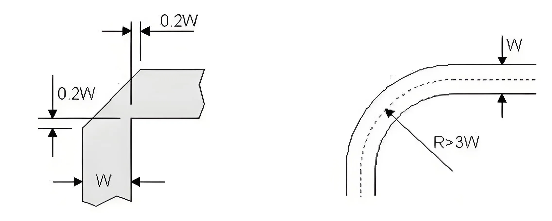
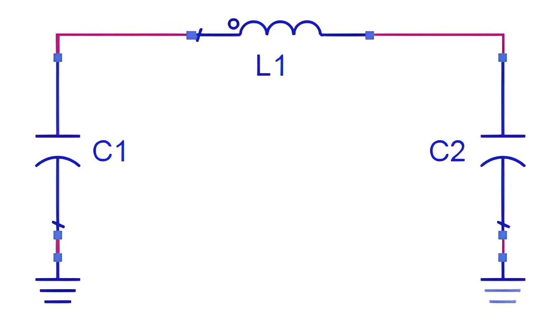
3. Mitigando o efeito capacitivo de pads grandes
Quando um bloco de componente grande é colocado em uma linha de microfita de 50 ohms, introduz capacitância parasita, interrompendo a impedância característica.
Solução: Combine dois métodos para melhoria: aumentar a espessura do substrato microstrip e criar uma folga (ou “recortar”) no plano de terra abaixo do bloco para reduzir o efeito capacitivo. A área livre deve estender-se pelo menos 20 mils além da almofada em todos os lados para fornecer isolamento suficiente.
4. PCB otimizado via design
Vias são uma fonte primária de descontinuidade de impedância devido aos seus parâmetros parasitas, que afetam a transmissão de sinal de alta velocidade.
* Via Fórmula de Capacitância Parasita:
C = (1.41 * εr * T * D1) / (D2 – D1)
*Onde T é a espessura da placa, D1 é o diâmetro da almofada, D2 é o diâmetro do anti-almofada, e εr é a constante dielétrica.*
* Via Fórmula de Indutância Parasita:
eu = 5.08 * h * [ln(4h / d) + 1]
Onde h é o comprimento da via (comprimento do esboço), e d é o diâmetro da broca.
-
Soluções:
-
Use a tecnologia via-in-pad para minimizar o tamanho do pad.
-
Otimize o diâmetro do anti-almofada (tipicamente 10-20 mils maior que o via pad).
-
Utilize a perfuração traseira para remover o stub não funcional.
-
Para sinais superiores a 1 GHz, realizar simulação e otimização usando ferramentas como HFSS e Optimetrics.
-
5. Otimização do conector coaxial passante
Conectores coaxiais passantes apresentam desafios de descontinuidade de impedância semelhantes aos de vias.
-
Solução: Aplique as mesmas técnicas de otimização usadas para vias, incluindo via-in-pad, fanout adequado, e otimização do diâmetro anti-almofada. As vias de aterramento devem ser colocadas uniformemente ao redor do conector (pelo menos 4) para garantir excelente continuidade do solo.
Tecnologias avançadas de fabricação de PCB para controle de impedância
A fabricação moderna de PCB oferece recursos aprimorados para controle de impedância:
-
Laminação Estritamente Controlada: Garante espessura uniforme do substrato com tolerâncias de ±10%.
-
Imagem direta a laser (Ldi): Fornece controle de largura de traço altamente preciso, com precisão de até ±0,2 mil.
-
Seleção de acabamento de superfície: Escolhendo o acabamento superficial correto (por exemplo, CONCORDAR, Prata de imersão) ajuda a minimizar seu impacto na impedância.
De acordo com IPC-6012D, tolerância de controle de impedância para classe 3 (alta confiabilidade) os produtos devem ser mantidos dentro de ±10%. Algumas aplicações exigentes exigem tolerâncias ainda mais rigorosas de ±5% ou mais rigorosas.
Verificação de projeto e recomendações de teste
Para garantir a continuidade da impedância, implementar as seguintes medidas:
-
Simulação de pré-layout: Execute cálculos de impedância usando ferramentas como SI9000 ou Polar Instruments.
-
Simulação pós-layout: Verifique os cálculos com parâmetros reais de empilhamento.
-
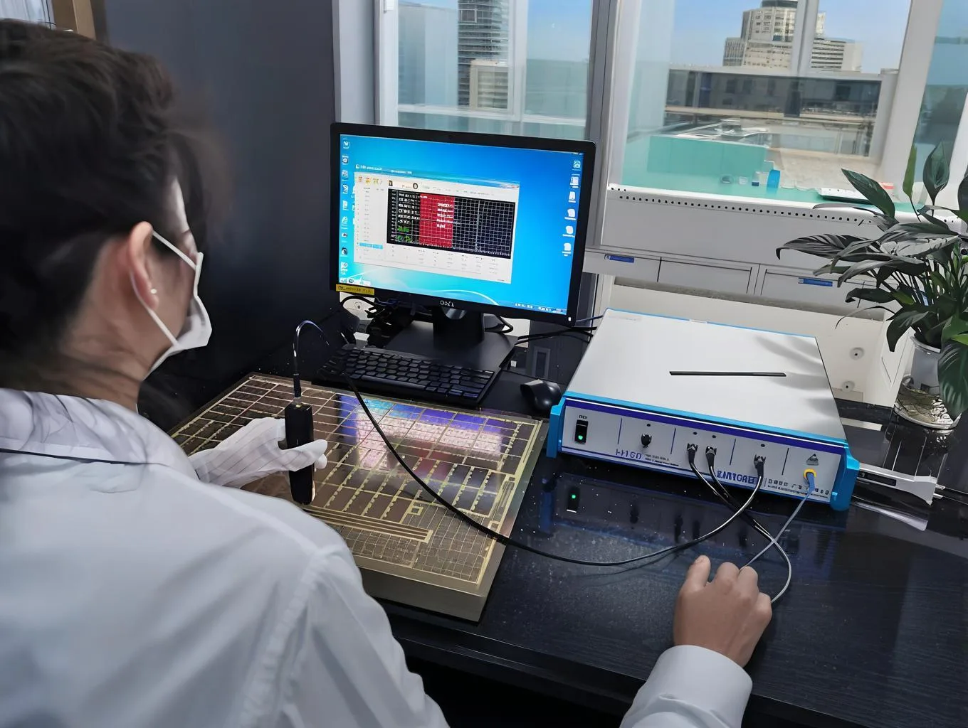
Teste TDR: Use um refletômetro no domínio do tempo para medir os valores reais de impedância após a produção.
-
Análise transversal: Audite periodicamente as capacidades da linha de produção, verificando a espessura dielétrica real e a largura do traço.
Conclusão
A descontinuidade de impedância no projeto de PCB é inevitável, mas o seu impacto pode ser minimizado através de metodologias de design científico e técnicas avançadas de fabrico. A chave para resolver este problema reside na compreensão das causas raízes das variações de impedância e na aplicação de estratégias de projeto apropriadas.. Para aplicações de alta velocidade e alta frequência, é aconselhável fazer parceria com fornecedores experientes como UGPCB, que possuem equipamentos de produção de última geração e ampla experiência em controle de impedância. Esses fornecedores são capazes de fornecer fabricação de PCB e Montagem PCBA serviços que atendem a rigorosos requisitos de desempenho.
Se você está procurando fabricação profissional de PCB e PCBA serviços, entre em contato conosco para um orçamento instantâneo e suporte técnico. Nossa equipe de engenharia fornecerá soluções abrangentes de impedância, desde o projeto até a produção, garantindo que seu produto atinja o desempenho ideal.

Na verdade, você faz com que sua apresentação pareça muito fácil, mas eu
acho que este tópico é algo que acho que nunca entenderia.
Parece muito complexo e extremamente amplo para mim.
Estou ansioso pela sua próxima postagem, vou tentar pegar o jeito!