
Introdução
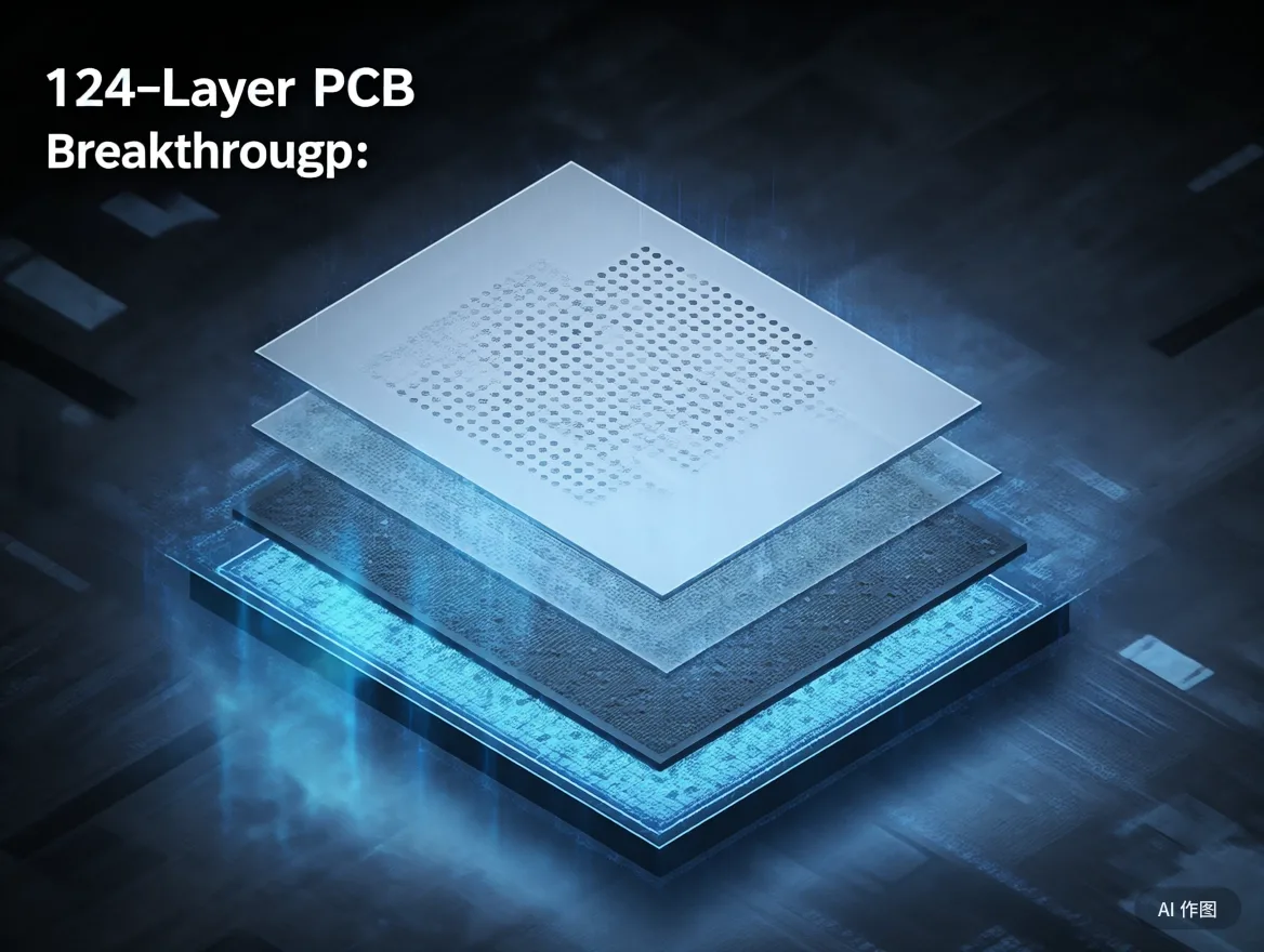
Impulsionado pela inteligência artificial (Ai) e computação de alto desempenho (HPC), A indústria global de eletrônicos está passando por uma revolução tecnológica centrada em “alta densidade, alta velocidade, e alta confiabilidade.” Em maio 2025, uma liderança Fabricante de placas de circuito impresso apresentou a primeira placa de circuito impresso comercial de 124 camadas do mundo, Quebrando a barreira da indústria de longa data de 108 camadas, mantendo a espessura padrão da placa de 7,6 mm. Este marco não apenas fornece suporte crítico de hardware para servidores de IA, Teste de semicondutor, e sistemas de defesa, mas também desbloqueia novas fronteiras na tecnologia de embalagens eletrônicas.
Quebrando a barreira de 108 camadas: Soluções de engenharia atrás de PCBs de 124 camadas
Inovações de fabricação de precisão
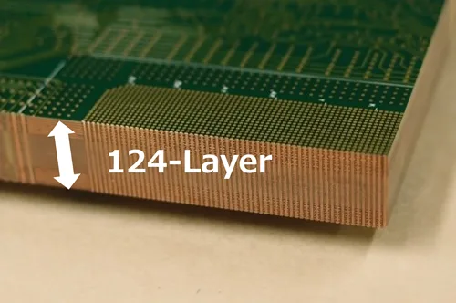
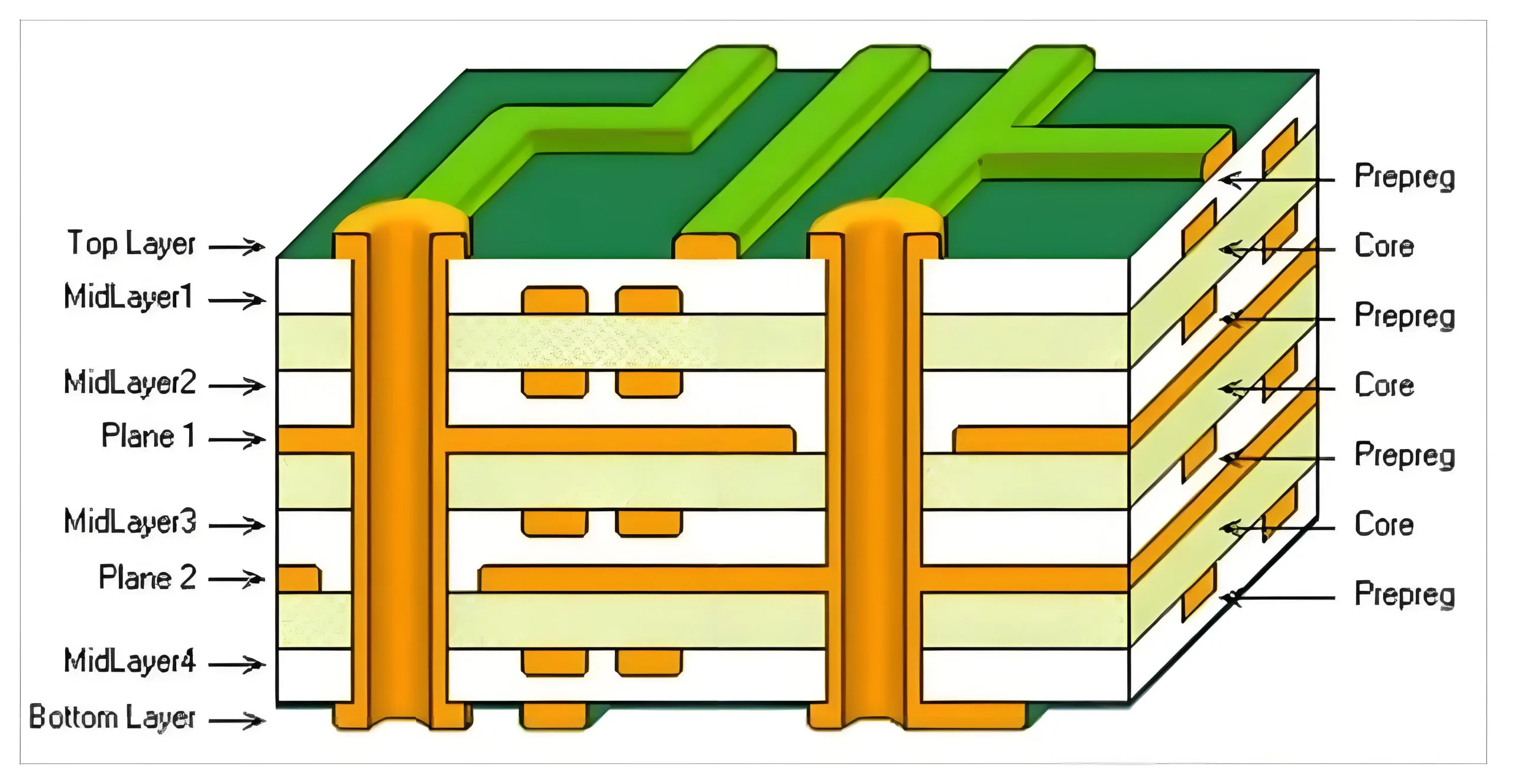
Tradicional Designs de PCB Face Mechanical and Thermal Limitações em 100 camadas devido a inconsistências de fluxo de resina, via colapso, e camada desalinhamento. O inovador PCB de 124 camadas alcança um 15% Aumentar a camada:
-
Dielétricos ultrafinos: 25Camadas µm usando materiais de baixa perda (por exemplo, Caiu 7) com ± 5% de controle de impedância para 112+ Sinais GHZ
-
3D otimização de interconexão: Matrizes de microvia que permitem densidade de sinal de 0,15 mm²/mm, Compacente com PCIE Gen6 e CXL 3.0 protocolos
Certificação de confiabilidade térmica
Certificado sob padrões MIL-STD-883G, A PCB de 124 camadas reside 1,000+ Ciclos térmicos (-55° C a 125 ° C.) enquanto mantém <1% perda de sinal em 80 Estresse mecânico da MPA - tornando -o ideal para aplicações aeroespaciais e de defesa.
Aplicações: Acelerando os avanços de hardware e semicondutores
Servidores de AI & Memória de alta largura de banda (HBM)
-
Densidade do sinal: 18% aumento do roteamento de pares diferenciais por camada
-
Gerenciamento térmico: Microvias cheias de cobre melhoram a condutividade térmica por 30%, crítico para aceleradores de 500W+ AI
Teste no nível da bolacha & 3Pacote D.
Ativa a precisão do alinhamento do sub-mícron (± 0,8 mm) e controle de atraso de sinal no nível do nível de picossegundos para módulos HBM empilhados-um divisor de águas para arquiteturas baseadas em chiplet.
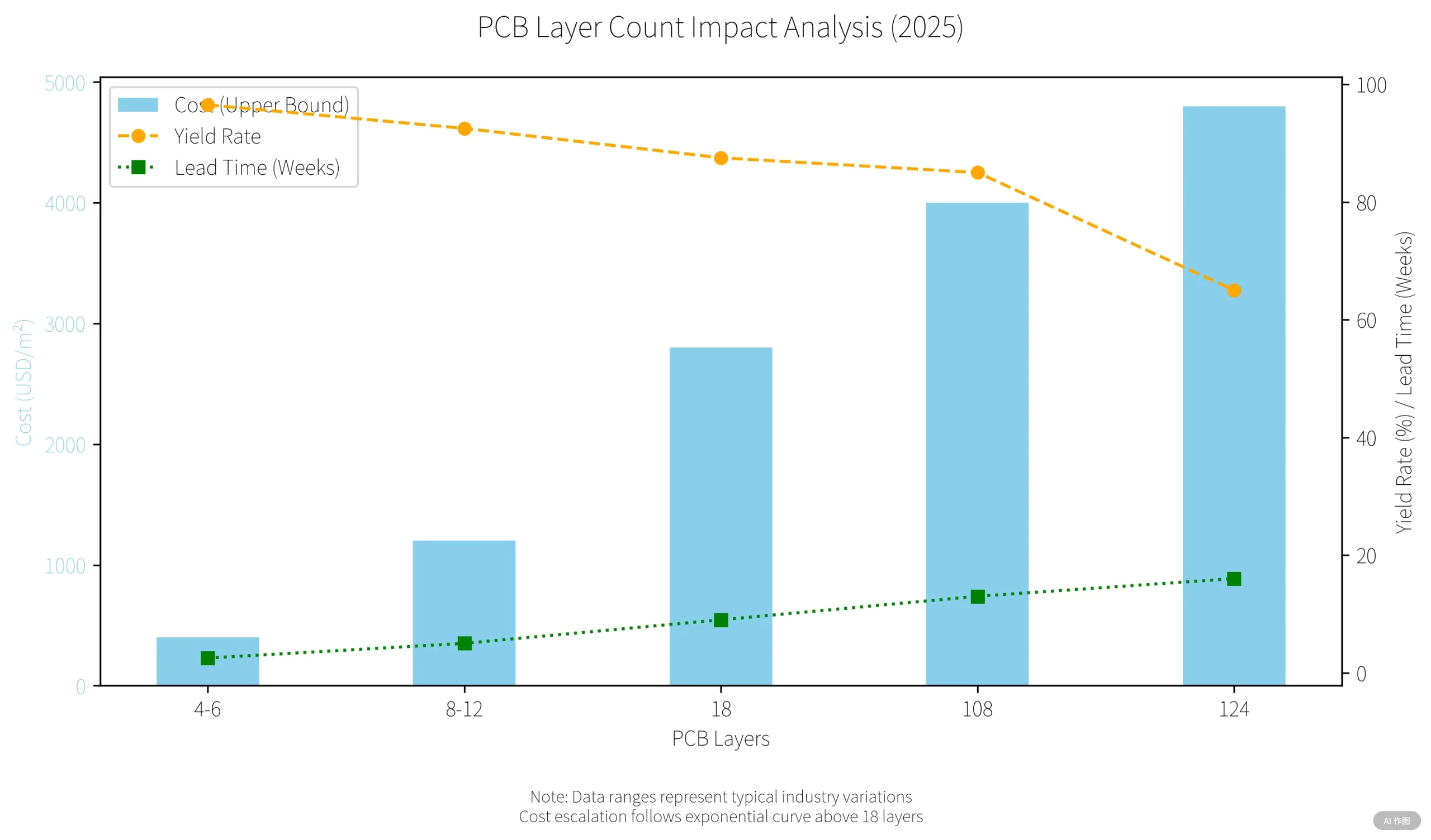
Desafios de custo & Roteiro de escalabilidade
Economia manufatureira
-
Custo do material: 4,800/m2(vs..3,200/m² para 108 camadas)
-
Taxas de rendimento: 65% (16-ciclo da semana) vs.. 85% para convencional IDH
-
Análise de falhas: Seção transversal destrutiva necessária para 20% de defeitos de estresse térmico
Caminhos de adoção industrial
-
Fabricação aditiva: Reduz as etapas de laminação por 40%
-
EDA orientado pela IA: Prevê através de pontos de estresse com 92% precisão, potencialmente aumentar os rendimentos para 75%
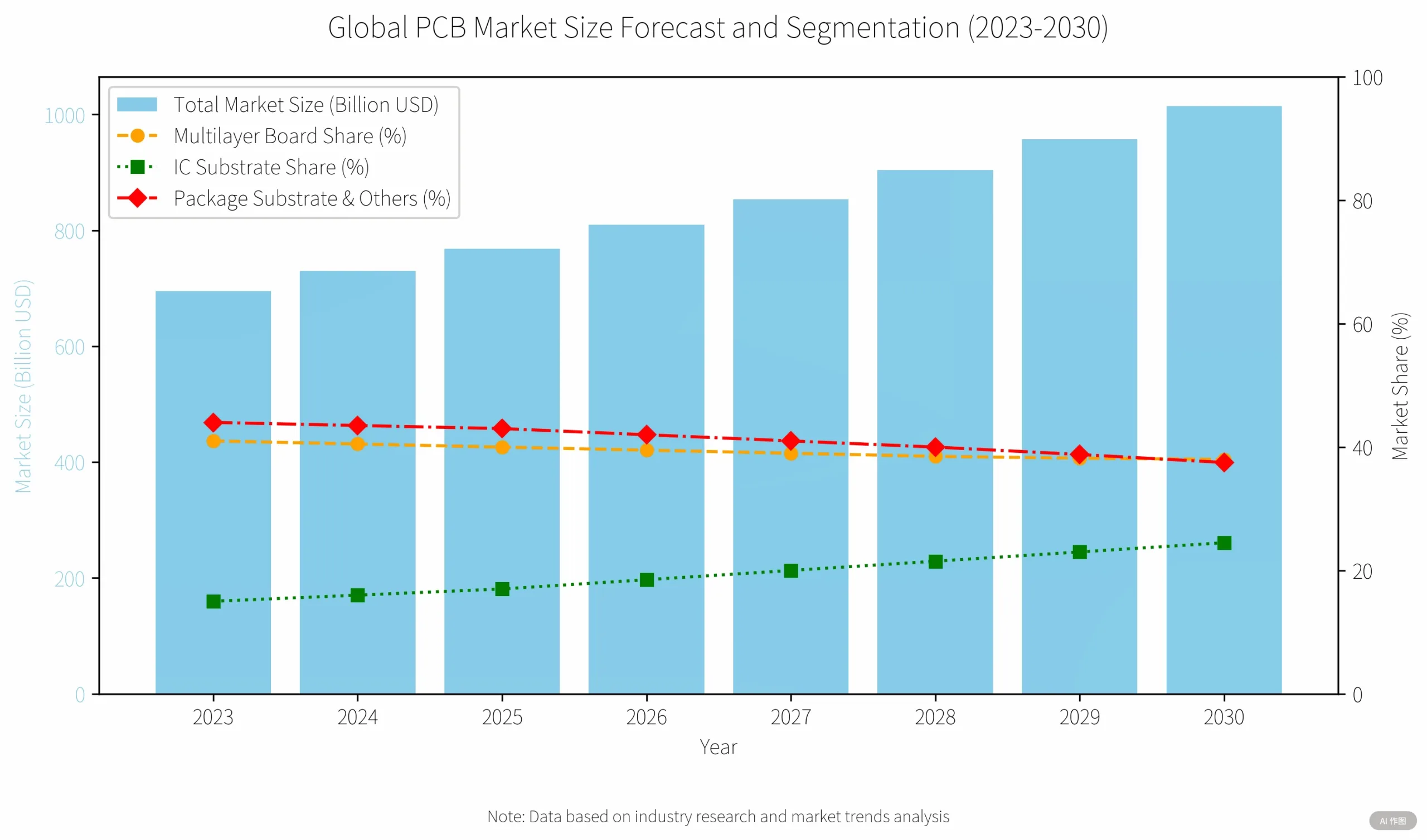
Perspectivas de mercado: $49B Transformação da indústria de PCB
Drivers de crescimento
-
Computação em nuvem: 70% CAGR em PCBs de servidor AI (Títulos citic 2026 projeção)
-
Dispositivos AI de borda: 30% Aumento de custos de PCB nos smartphones de próxima geração (Dados da cadeia de suprimentos da Apple)
-
Tendências de localização: Fabricantes chineses gostam UGPCB direcionando 3,6m m²/ano de capacidade para substratos avançados
Conclusão: Inovação prática sobre registros de contagem de camadas
Embora não supere o protótipo de 129 camadas de Denso (2012), Este PCB de 124 camadas define um novo benchmark comercial através:
-
Espessura padronizada (7.6milímetros) Para compatibilidade com versões anteriores
-
Confiabilidade da MIL-especificação em 85% de custos de protótipo
-
Processos de fabricação escaláveis
À medida que a computação quântica e 6G surgem, A inovação em PCB priorizará a densidade funcional sobre a contagem de camadas - uma mudança crucial para o progresso tecnológico sustentável.
