
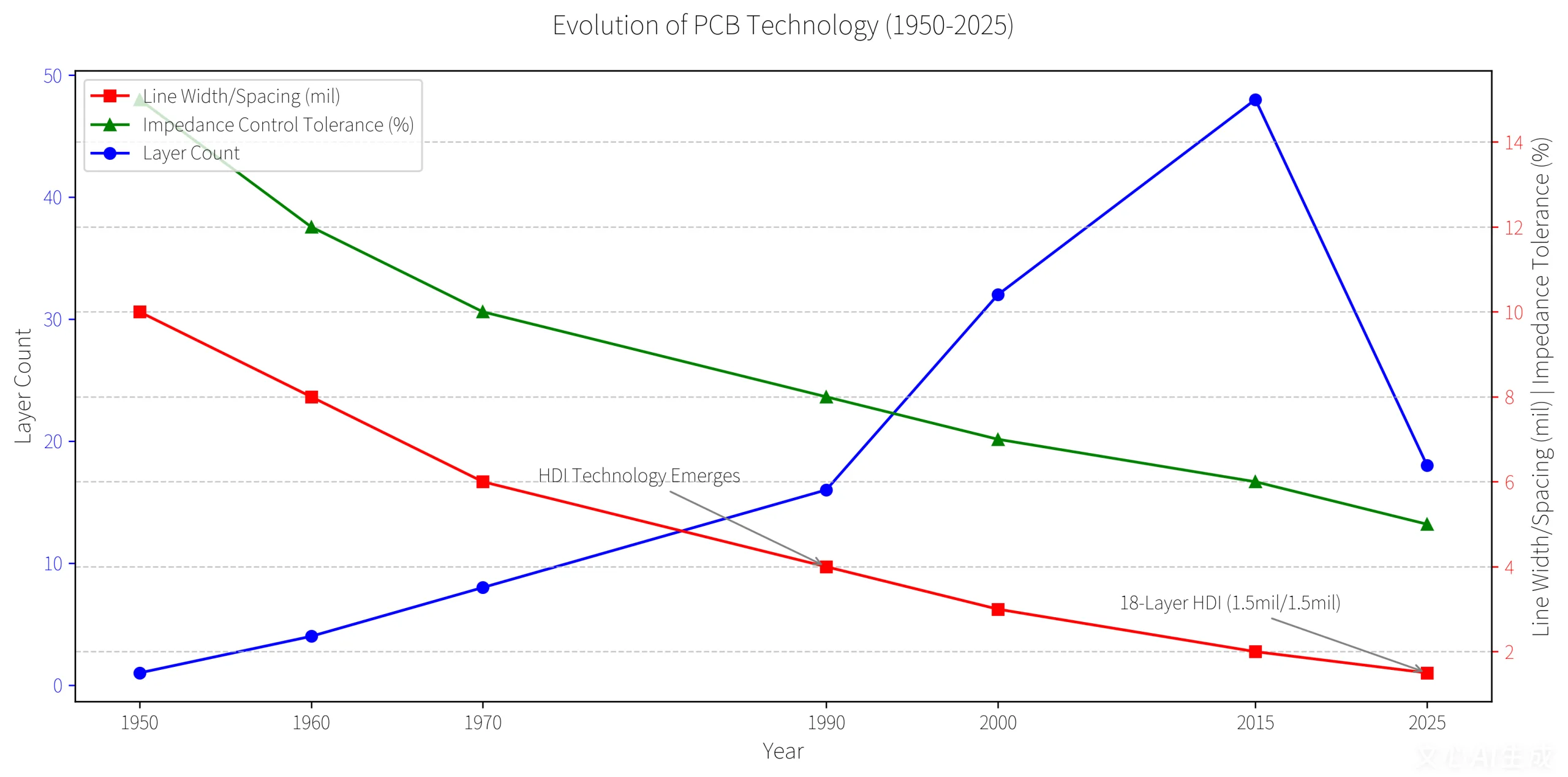
1. PCB Technology Evolution and Innovation Drivers
O PCB (Placa de circuito impresso) serve como o “mother of electronic products,” enabling mechanical fixation and electrical connection of components through copper traces and pads. Modern PCBs have evolved from single-layer boards to high-density interconnect (IDH) and multi-layer boards, driven by demands for high performance, miniaturização, e confiabilidade.
Key Market Drivers:
- AI server demand surged 60% YoY in 2025, boosting HDI and multi-layer PCB adoption.
- Automotive electronics penetration, especially in EVs, fuels high-reliability PCB growth.
- UGPCB’s 10-layer first-order PCB reduces signal loss by 42% using 2mil traces and laser microvia technology.
Technical Breakthroughs:
- Trace width/spacing as low as 1.5mil/1.5mil (Média da indústria: 3mil).
- Impedance control tolerance of ±5% (Exceeds industry standards by 10%).
2. PCB Classification and Applications
2.1 Layer-Based Classification
Single-Layer PCBs: Simple designs (por exemplo, toys, power adapters).
Double-Layer PCBs: Uses vias for interconnection; ideal for routers and home appliances.
Multi-Layer PCBs (3+ Camadas): High-density designs for smartphones, automotive systems, e controladores industriais.
2.2 Material & Process-Based Classification
Rigid PCBs: FR-4 substrate for fixed-form devices (phones, TVs).
PCBs flexíveis (CPF): Polyimide-based for bendable applications (screen cables, wearables).
Rigid-Flex PCBs: Combines rigid and flexible sections for complex assemblies (drones, dispositivos médicos).
3. Application-Specific Requirements
3.1 Eletrônicos de consumo
- Smartphones: 12-layer rigid PCBs for CPUs, câmeras, and RF modules.
- Laptops: 6-10 layer boards for CPUs; FPCs for battery connections.
3.2 Eletrônica Industrial
- PLC Controllers: 4-6 layer PCBs with EMC resistance for motor control.
- Sensores: Double-layer boards with stable signal transmission in harsh environments.
3.3 Eletrônica Automotiva
- EV Battery Management: Multi-layer PCBs for voltage/temperature monitoring.
- ADAS Systems: High-reliability boards with millisecond-level response.
3.4 High-End Applications
- 5G Estações básicas: 8-12 layer RF boards for high-frequency signal integrity.
- Dispositivos médicos: Multi-layer PCBs with biocompatible materials for ECG machines.
4. Market Data and Growth Projections
- Global PCB market: 155.38B by 2037.
- Placas de IDH: 33.4% market share by 2037, driven by smartphones and AI servers.
- Automotive PCBs: 18.79B by 2035 (Cagr 5.5%).
China’s Dominance: Accounts for 50% of global production; high-end PCBs to reach 40% share by 2025.
5. PCB and SMT Synergy
PCB design and SMT (Tecnologia de montagem em superfície) are interdependent:
- PCBs provide precise solder pad layouts for SMT components (por exemplo, 0402 resistores: 0.4mm×0.2mm).
- SMT enables high-density assembly, such as BGA chips on smartphone PCBs.
UGPCB’s Advantage: LPKF laser imaging systems achieve ±25μm alignment accuracy, critical for HDI production.
6. Future Challenges and Trends
Cost Pressures:
- Copper prices up 15% em 2025;Laminado revestido de cobre (Ccl) costs rose 8-12%.
- SMEs face margin compression, accelerating industry consolidation.
Technological Shifts:
- Rising demand for 8-16 layer PCBs and IC substrates (market size: $45B by 2025).
- Low-power, high-thermal-conductivity materials for eco-friendly designs.
Expansão global:
- PCB manufacturers investing in Southeast Asia (Vietnã, Tailândia) for cost efficiency and tariff avoidance.
Conclusão
The PCB industry remains pivotal to global electronics, driven by AI, automotivo, and 5G innovations. Companies must prioritize technical upgrades, supply chain diversification, and green manufacturing to thrive amid cost volatility and regional competition.
