

Introdução ao 6 Camada PCB
O 6 Layer PCB is a sophisticated electronic component designed for high-performance applications requiring complex circuitry. It consists of six layers of conductive material, typically copper, separados por camadas isolantes. This multilayer structure allows for greater functionality and compactness compared to single or double-sided PCBs.
O que é a 6 Camada PCB?
UM 6 Camada PCB, ou Placa de circuito impresso, is an advanced electronic substrate that features six layers of conductive pathways embedded within insulating layers. These layers are meticulously arranged to create intricate circuit designs suitable for demanding electronic applications. The additional layers provide enhanced signal integrity, distribuição de energia, and thermal management capabilities.
Requisitos de design
Designing a 6 Layer PCB involves several critical considerations:
- Seleção de material: Common materials include S1141, S1000, e 370RH, chosen based on their electrical properties and compatibility with the manufacturing process.
- Layer Stackup: Determines the arrangement of signal and ground planes, crucial for minimizing crosstalk and ensuring reliable signal transmission.
- Espessura do Cobre: Typically specified as 1/H/H/H/H1 OZ, indicating varying thicknesses across different layers to optimize performance and cost.
- Tratamento de superfície: Options like Immersion Gold or OSP (Organo-Silicon Protection) are applied to protect the copper surfaces and enhance solderability.
Como funciona?
O 6 Layer PCB functions by providing a platform for electrical components to be interconnected through a series of conductive paths etched onto its surface. Each layer contains specific patterns of copper traces that form circuits when connected via plated through-holes or vias. The multiple layers enable more complex circuit designs without increasing the board’s footprint, making it ideal for modern electronic devices where space is limited.
Aplicações
Due to their complexity and capability to handle high-speed signals with minimal interference, 6 Layer PCBs are widely used in consumer electronics such as smartphones, comprimidos, notebooks, and other portable devices. They are also found in automotive electronics, Equipamento médico, and industrial controls where reliability and performance are paramount.

Classificação
6 Layer PCBs can be classified based on several factors:
- Por material: As mentioned, they may use S1141, S1000, or 370HR depending on the required characteristics.
- Por aplicação: General-purpose or specialized for specific industries like telecommunications, aeroespacial, or defense.
- Por tratamento de superfície: Different finishes like Immersion Gold or OSP cater to various environmental conditions and soldering processes.
Materiais utilizados
The primary materials used in manufacturing 6 Layer PCBs include:
- Material base: Often fiberglass-reinforced epoxy resins (FR-4), which offer excellent mechanical strength and thermal stability.
- Folha de cobre: Varying thicknesses are used to balance conductivity and cost-effectiveness.
- Máscara de solda: Typically green in color, Protege os traços de cobre da oxidação e curtos -circuitos acidentais.
- Silk Screen: A white coating used for labeling components and providing instructions for assembly.
Características de desempenho
Key performance attributes of a 6 Layer PCB include:
- Integridade do sinal: Enhanced by strategic layer placement and grounding schemes.
- Gerenciamento térmico: Improved heat dissipation due to larger copper areas and potentially thicker boards.
- Força mecânica: Multilayer construction adds rigidity, reducing the risk of damage during handling or operation.
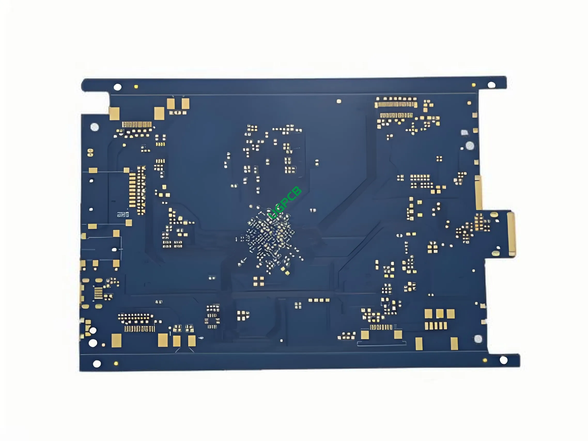
Composição estrutural
Estruturalmente, um 6 Layer PCB comprises:
- Camadas condutivas: Six layers of copper traces separated by dielectric materials.
- Camadas isolantes: Prevenir shorts elétricos entre camadas condutoras.
- Vias: Conductive holes that connect different layers, allowing vertical integration of circuits.
Características distintas
Some notable features of a 6 Layer PCB are:
- Alta densidade: Allows for complex circuit designs within a compact form factor.
- Confiabilidade: Multilayer design improves resistance to electromagnetic interference (EMI).
- Versatilidade: Suitable for a wide range of applications due to customizable layer configurations and material choices.
Processo de Produção
The manufacturing process of a 6 Layer PCB involves several steps:
- Design e layout: Usando software especializado para criar o padrão de circuito.
- Preparação de Materiais: Cortando materiais base para o tamanho e as superfícies de limpeza.
- Laminação: Empilhar e unir camadas individuais sob calor e pressão.
- Gravura: Removendo o excesso de cobre para formar os caminhos de circuito desejado.
- Revestimento: Adicionando uma fina camada de metal a vias e áreas de cobre expostas.
- Aplicação de máscara de solda: Applying the green coating to protect traces.
- Silk Screen Printing: Adding text and symbols for component placement.
- Inspeção Final: Garantir a qualidade e funcionalidade antes do envio.
Casos de uso
Common scenarios where a 6 Layer PCB might be employed include:
- Aplicações de interconexão de alta densidade em dispositivos móveis.
- Sistemas de comunicação avançada que requerem baixa perda de sinal.
- Instrumentos médicos portáteis que precisam de desempenho confiável em ambientes severos.
- Eletrônicos automotivos exigindo robustez e longevidade.
Resumindo, o 6 Layer PCB represents a significant advancement in printed circuit board technology, Oferecendo complexidade e desempenho incomparáveis para aplicações eletrônicas modernas. Sua flexibilidade de design, combinado com integridade e durabilidade do sinal superior, makes it an essential component in the development of next-generation consumer electronics and beyond.


