
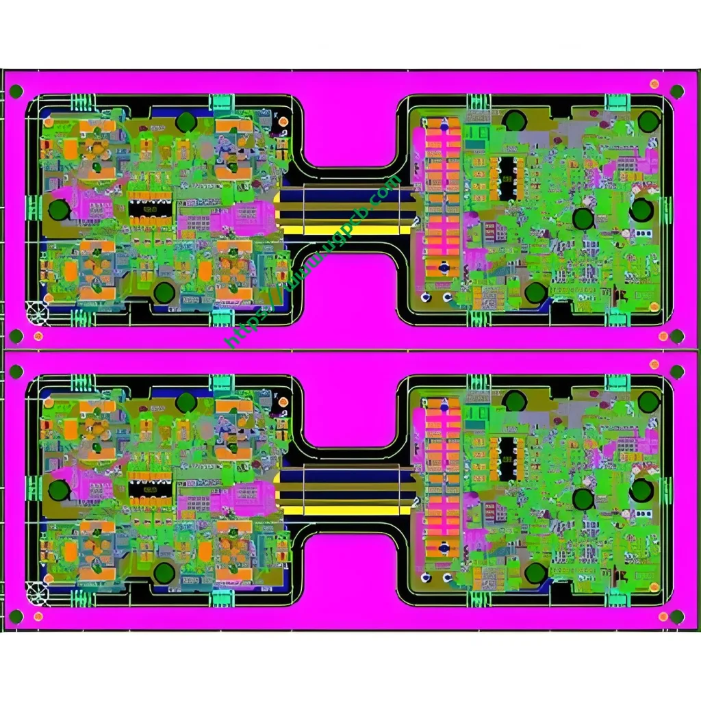
Definition of HDI PCB
Interconexão de alta densidade (IDH) is simply a PCB with a higher number of interconnects in the smallest footprint. This leads to miniaturization of the circuit board. Components are placed closer together and board space is significantly reduced, but functionality is not compromised.
More precisely, a PCB with an average of 120 para 160 pins per square inch is considered an HDI PCB. HDI designs combine dense component placement and versatile routing. HDI popularized microporous technology by implementing microvias, buried vias, and blind vias. Reduced drilling of copper is a feature of HDI designs.
Advantages of HDI PCB
Versatilidade Extraordinária
As placas HDI são ideais quando o peso, espaço, confiabilidade, e desempenho são as principais preocupações.
Design Compacto
A combinação de cego, enterrado, e micro vias reduzem os requisitos de espaço na placa.
Melhor integridade de sinal
HDI utiliza tecnologia via-in-pad e blind via. This helps keep components close to each other, reduzindo comprimentos do caminho do sinal. A tecnologia HDI remove stubs de passagem, thus reducing signal reflections, thereby improving signal quality. Portanto, it significantly improves signal integrity due to shorter signal paths.
Alta confiabilidade
A implementação de vias empilhadas torna estas placas uma superbarreira contra condições ambientais extremas.
Econômico
A funcionalidade de uma placa passante padrão de 8 camadas (PCB padrão) can be reduced to a 6-layer UGPCB board without compromising the quality.


