การแนะนำ: Challenges and Opportunities in High-Density PCB Design
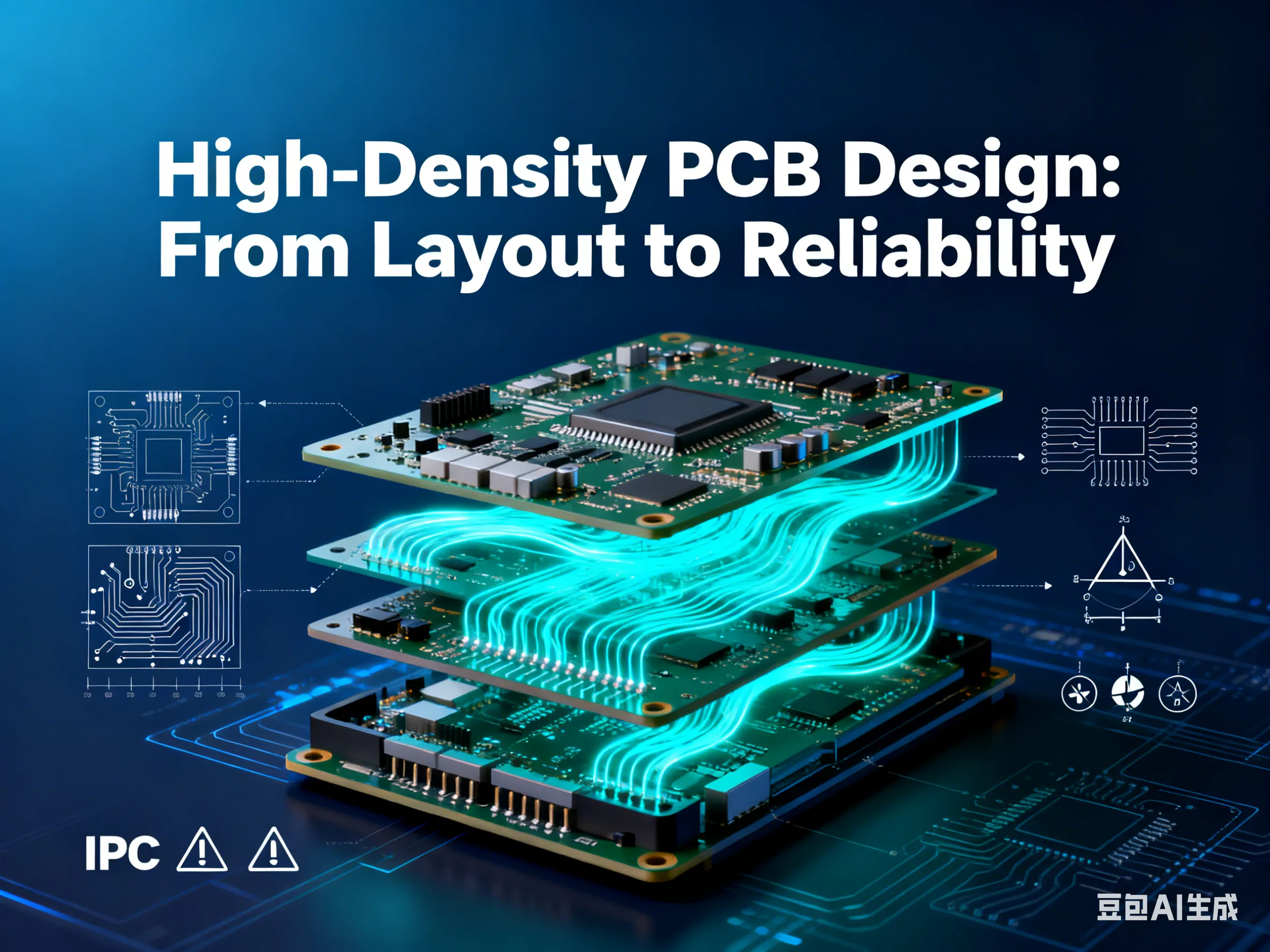
As electronic products evolve toward higher speeds and greater integration, การออกแบบ PCB has transformed from simple connection tasks into complex system engineering. A board with 8000 PINs often involves multiple high-speed interfaces and power management units, where improper design can lead to ความสมบูรณ์ของสัญญาณ issues and thermal failures. According to IPC market reports, the global การเชื่อมต่อระหว่างกันที่มีความหนาแน่นสูง (HDI) พีซีบี market grew by over 15% ใน 2022, highlighting the industry’s demand for specialized design expertise.
During initial design stages, engineers must comprehensively analyze schematic diagrams and hardware guidance documentation to ensure optimization of high-speed signals and power paths. This approach not only enhances พีซีบี ความน่าเชื่อถือ but also helps quickly identify reliable ซัพพลายเออร์ PCB and obtain accurate quotations in a competitive market.

PCB Design Preparation: Signal Analysis and Power Planning
Upon receiving the schematic, the first step is a quick review to identify typical พีซีบี circuits and high-speed signals such as LPDDR4, PCIE 3.0, and HDMI. Design guidelines provided by hardware engineers are crucial; if missing, proactively request and document these key points. ตัวอย่างเช่น, high-speed signals are particularly sensitive to impedance and reference planes, and overlooking these details could lead to signal attenuation of up to 20% (based on IPC-2141 standard).
Creating a power tree is an essential next step. This tree clearly illustrates the current carrying conditions of each branch, facilitating optimization of the power distribution network. Assuming a board contains multiple LDO and DC-DC converters, current carrying capacity calculations must consider temperature rise factors according to IPC-2152 standard. ตัวอย่างเช่น, a typical 12V input, 3.3V output DC-DC module’s current carrying capacity at 25°C ambient temperature can be estimated using the formula I = k·A^0.7, where k is a material constant (โดยทั่วไป 0.024 for copper foil) and A is the cross-sectional area (in square millimeters). This ensures power path reliability and avoids overload risks.
During signal analysis, boards may include high-speed interfaces like LPDDR4, PCIE 3.0, and USB 3.0, alongside analog audio and LVDS signals. High-speed signals typically require strict การควบคุมความต้านทาน, while analog sections need isolation to reduce noise. This modular analysis allows designers to pre-plan resources, improving subsequent เค้าโครง PCB ประสิทธิภาพ.
Stack-up Planning and Impedance Control: Building a Robust PCB Foundation
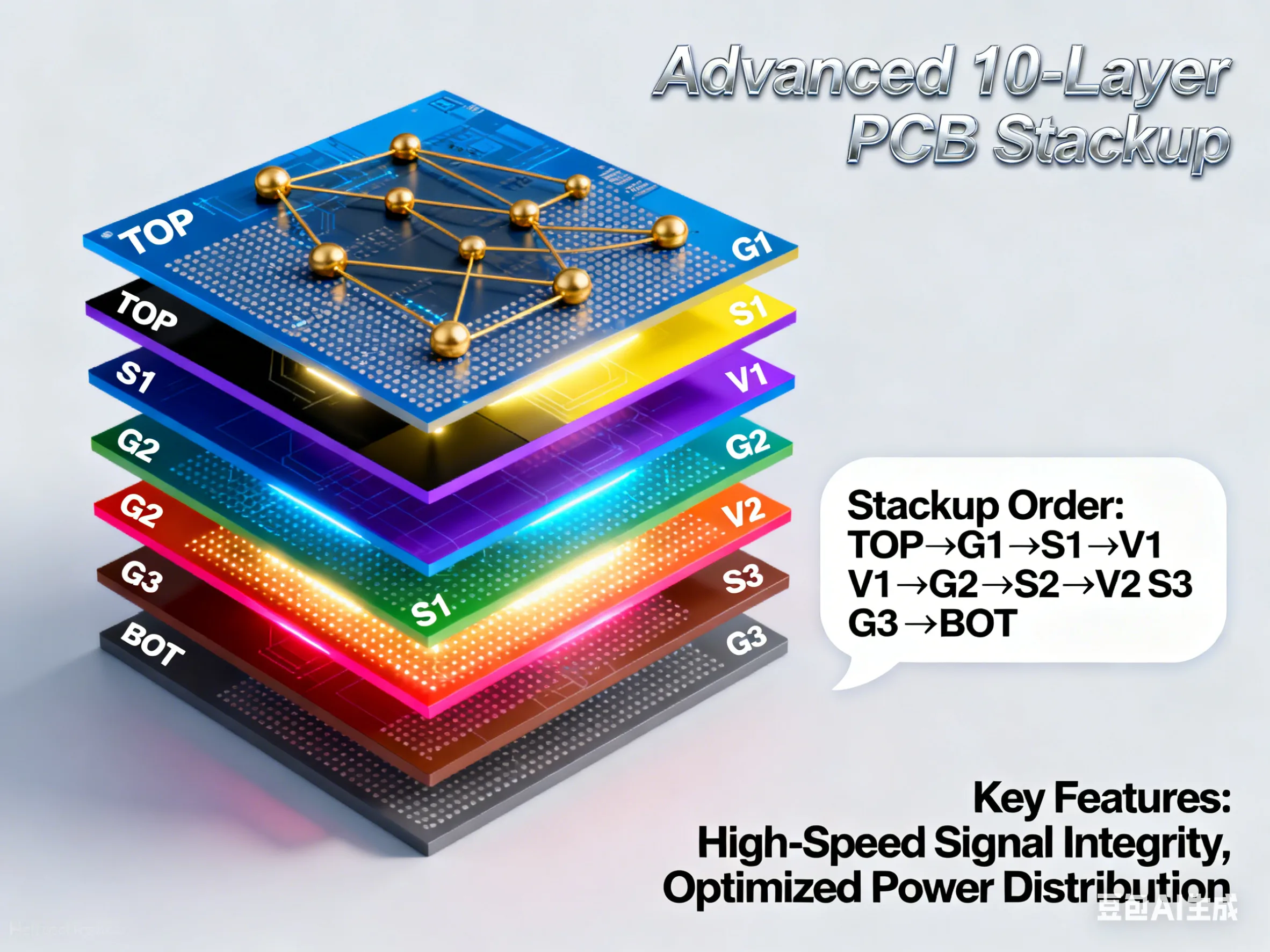
Stack-up planning is central to high-density PCB design, directly impacting ความสมบูรณ์ของสัญญาณ and EMC performance. For an 8000 PIN board, a 10-layer structure (such as TOP/G1/S1/V1/G2/S2/V2/S3/G3/BOT) effectively balances cost and performance. The principle is to ensure each signal layer has a corresponding ground plane as reference, reducing crosstalk and impedance discontinuities. According to IPC-2221 standard, typical FR-4 material has a dielectric constant of approximately 4.5. When calculating microstrip impedance, the commonly used formula is:
Z₀ = 87/√(εr + 1.41) × ln(5.98ชม/(0.8W + T))
Where Z₀ is the characteristic impedance (in Ω), εr is the dielectric constant, H คือความหนาของอิเล็กทริก (in mils), w is the trace width (in mils), และ T คือความหนาของทองแดง (in mils). In practical design, collaborate with your ผู้ผลิต PCB, providing impedance requirements (such as 50Ω single-ended or 100Ω differential) for them to calculate specific trace width and spacing. ตัวอย่างเช่น, LPDDR4 signals might require a configuration of 4mil trace width and 4mil spacing to match target impedance.
This planning approach not only improves signal quality but also reduces late-stage modifications, accelerating the PCBA production วงจร. Statistics show that designs following IPC stack-up guidelines can reduce signal loss by over 30% (data source: IPC-6012 standard).

PCB Layout Strategies: Combining Modularization and Design Review
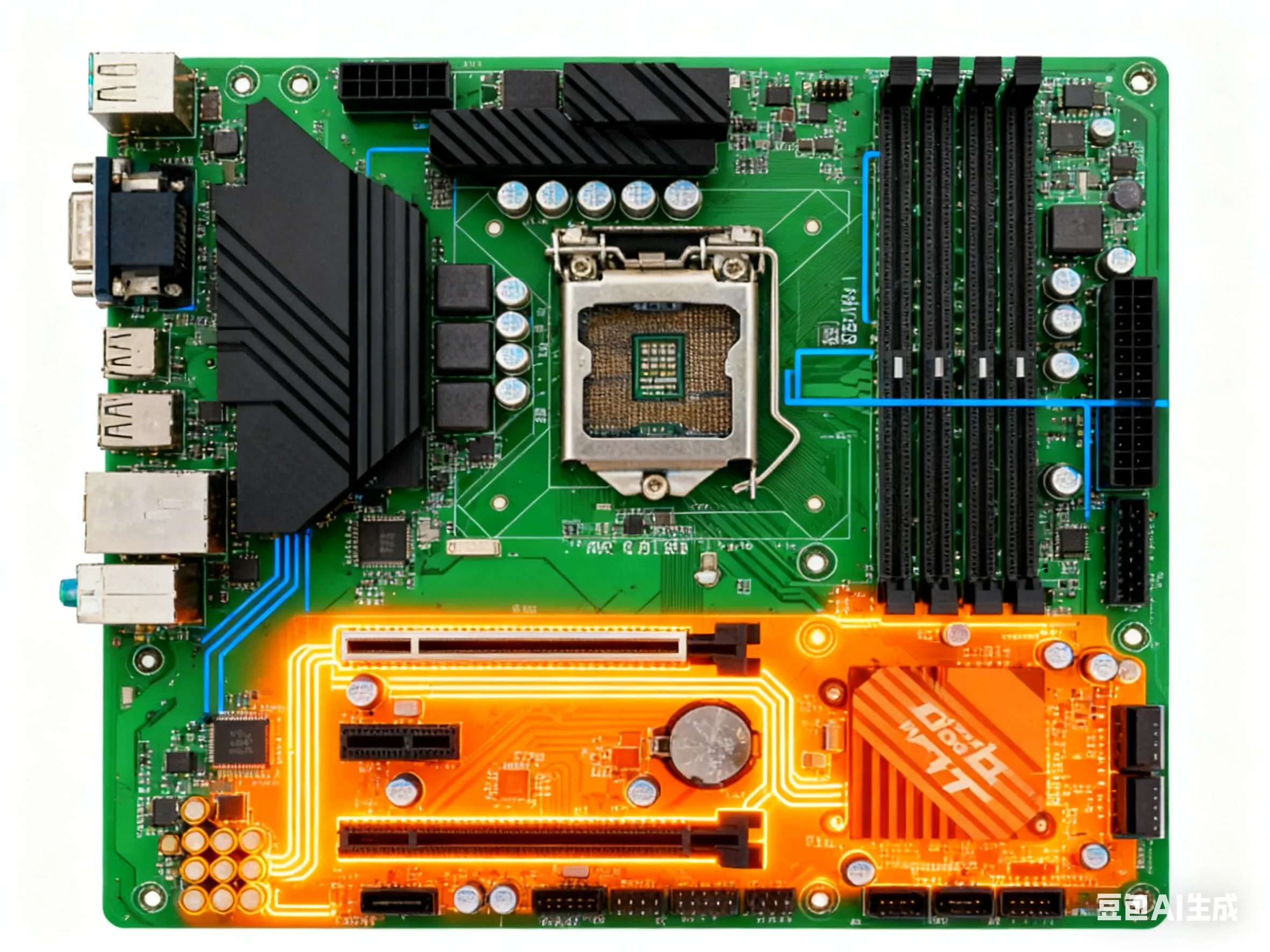
เค้าโครง PCB represents the artistic aspect of PCB design, requiring adherence to principles like separating high and low voltages and isolating digital and analog circuits. อันดับแรก, confirm external connector positions as they influence overall routing flow. แล้ว, ดำเนินการ modular layout: process each subunit (such as FPGA chips or power modules) individually before placement according to signal flow direction. ตัวอย่างเช่น, high-speed signals like PCIe 3.0 should be positioned close to connectors, while analog audio sections need distancing from digital areas to reduce coupling noise.
Placement of heat-generating components also demands attention. According to Newton’s law of cooling, heat dissipation efficiency relates to surface area and airflow, so reserve thermal dissipation channels during layout. In typical designs, use the thermal resistance formula from IPC-2221, Rθ = ΔT/P, where Rθ is thermal resistance (in °C/W), ∆T คืออุณหภูมิที่เพิ่มขึ้น, and P is power dissipation. ตัวอย่างเช่น, a chip dissipating 2W with a thermal resistance of 50°C/W may experience a 100°C temperature rise, necessitating thermal vias or copper foil expansion.
Upon layout completion, conducting a design review with hardware engineers to confirm critical aspects is mandatory. This step prevents rework and improves first-pass success rates. Industry practice has proven that modular layout can reduce board layout time by 20% (based on IPC design benchmark data).

PCB Routing Implementation: From Rule Setup to DRC Verification
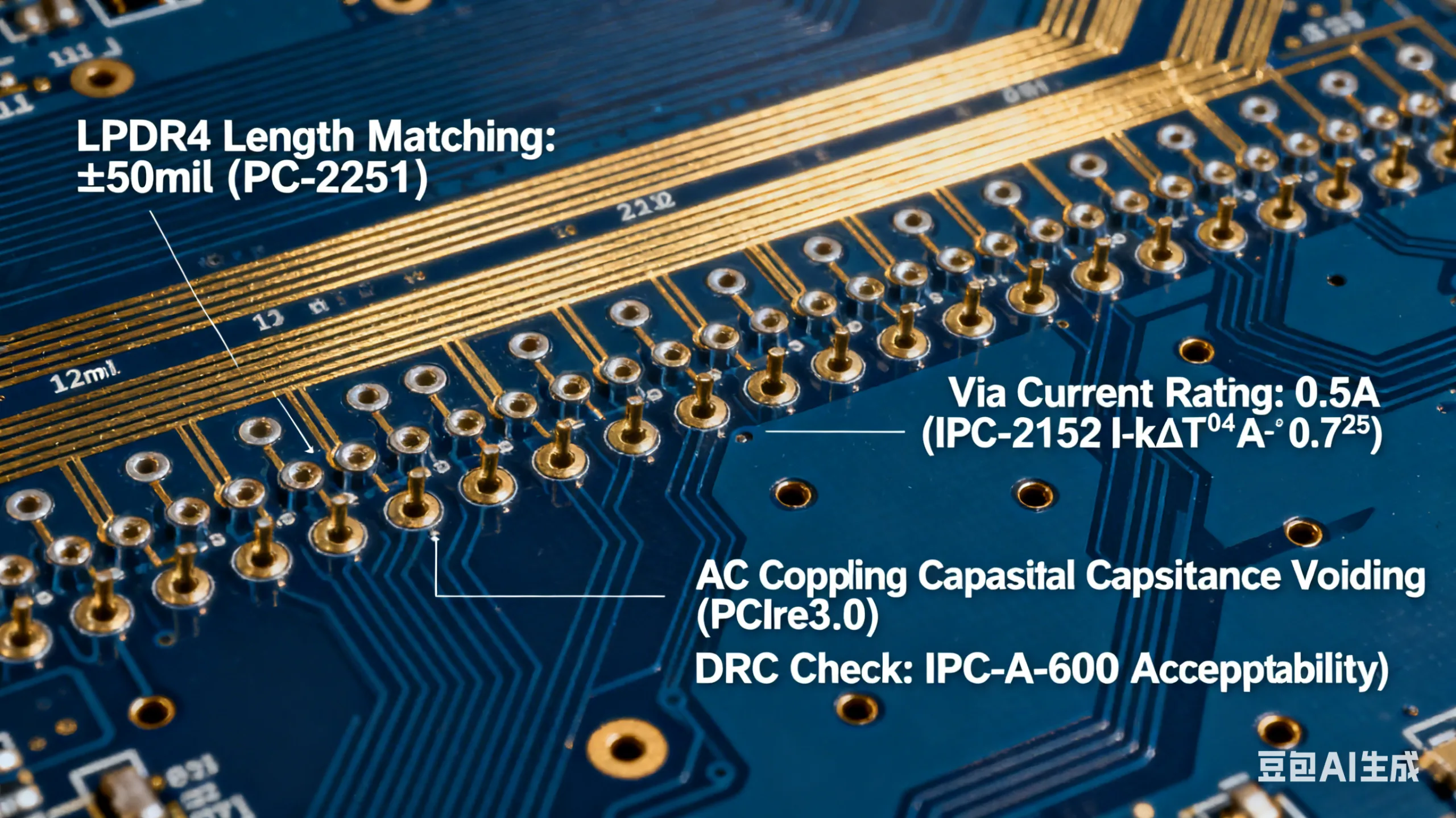
Before การกำหนดเส้นทาง PCB, setting up design rules is fundamental, encompassing minimum clearances, via sizes, and high-speed constraints. ตัวอย่างเช่น, for LPDDR4 signals, set length matching rules with deviations controlled within ±50mils (referencing IPC-2251 standard). แล้ว, place vias before routing: ensure vias for all modules are arranged orderly, considering routing clearance and copper integrity. โดยทั่วไป, use 12mil vias, with each via carrying approximately 0.5A, based on IPC-2152 current carrying formula I = k·ΔT^0.44·A^0.725, where ΔT is the allowable temperature rise (in °C) and A is the cross-sectional area (in circular mils). This ensures power paths won’t bottleneck due to insufficient vias.
The routing principle is “short, straight, and minimal vias.” High-speed traces require attention to reference plane integrity and should incorporate accompanying ground vias to reduce return path impedance. Proper clearance handling under AC coupling capacitors is also critical; ตัวอย่างเช่น, in PCIe 3.0 การออกแบบ, the clearance area should extend beneath the capacitor to reduce parasitic capacitance. After completing the routing, ดีอาร์ซี (Design Rule Check) serves as the final checkpoint. Use a comprehensive checklist covering acceptability criteria from IPC-A-600 standard, such as minimum pad size and copper coverage.

บทสรุป: Optimizing Design to Enhance PCBA Value
Through this systematic approach, high-density PCB design สำหรับ 8000 PIN boards can not only meet performance requirements but also reduce production costs. As a การออกแบบ PCB expert, I recommend collaborating with reliable ซัพพลายเออร์ PCB during early design stages to obtain custom quotations and optimize material selection and lead times. ในที่สุด, professional design not only accelerates time-to-market but also provides competitive advantages for your products.
If you require further PCB or PCBA design สนับสนุน, please contact professional PCB suppliers for detailed quotations and consulting services. Share knowledge and advance together—let’s continue breaking new ground in electronic design!
 โลโก้ UGPCB

