
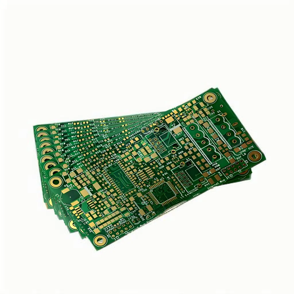
What is a 10Layers ENIG Board?
A 10-layer ENIG (ทองคำแช่นิเกิลแบบไม่ใช้ไฟฟ้า) board is an advanced multilayer printed circuit board (พีซีบี) with ten layers of conductive material, โดยทั่วไปแล้วทองแดง, คั่นด้วยเลเยอร์ฉนวน. ที่ “เห็นด้วย” refers to the surface treatment applied to the copper traces, which involves electroless nickel and immersion gold plating. This type of พีซีบี is designed for high-density and complex electronic applications.

ข้อกำหนดการออกแบบ
Designing a 10-layer ENIG board involves several key considerations:
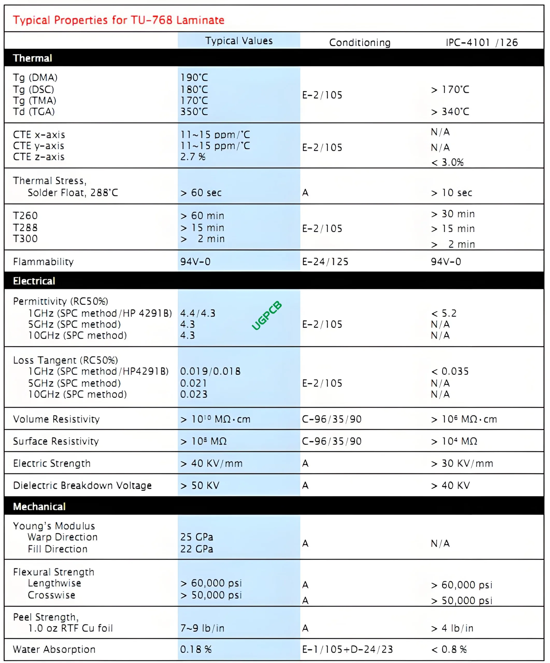
- วัสดุ: Made from TU-768, a high-performance composite material known for its excellent electrical properties and durability.
- จำนวนเลเยอร์: Consists of ten layers, allowing for intricate and dense circuit designs.
- ความหนาของทองแดง: Ranges from 2OZ to 3OZ, providing robust conductivity for high-power applications.
- การรักษาพื้นผิว: Features immersion gold plating, which offers excellent solderability and corrosion resistance.
- ติดตามและพื้นที่: Minimum trace and space are set at 3mil (0.075มม), enabling fine details in the circuit design.
มันทำงานอย่างไร?
The 10-layer ENIG board functions by providing multiple layers of conductive pathways, คั่นด้วยเลเยอร์ฉนวน, to interconnect electronic components. The immersion gold surface treatment ensures reliable soldering and long-term protection against oxidation and wear.
การใช้งาน

เนื่องจากความซับซ้อนและความน่าเชื่อถือของพวกเขา, 10-layer ENIG boards are widely used in various high-end electronic applications including:
- Aerospace and defense systems
- High-speed networking equipment
- Advanced telecommunication devices
- Medical imaging equipment
การจำแนกประเภท
10-layer ENIG boards can be classified based on several factors:
- โดยวัสดุ: Most commonly made from TU-768 due to its balance of cost, ความแข็งแกร่ง, และคุณสมบัติไฟฟ้า.
- โดยความหนาของทองแดง: แตกต่างจากน้ำหนักเบา (2ออนซ์) ถึงเฮฟวี่เวท (3ออนซ์) ขึ้นอยู่กับความต้องการของแอปพลิเคชัน.
- โดยการรักษาพื้นผิว: Features immersion gold plating, which provides excellent solderability and corrosion resistance.
วัสดุที่ใช้
The primary materials used in manufacturing 10-layer ENIG boards include:
- TU-768: ลามิเนตอีพ็อกซี่เสริมแก้วที่ให้ความแข็งแรงเชิงกลที่ยอดเยี่ยมและความเสถียรทางความร้อน.
- ทองแดง: ใช้สำหรับชั้นนำไฟฟ้า, ด้วยความหนาแตกต่างกันไปตามข้อกำหนดการออกแบบ.
- หน้ากากบัดกรี: Typically green or white, ช่วยปกป้องร่องรอยทองแดงจากการออกซิเดชั่นและการลัดวงจรโดยไม่ตั้งใจ.
- ทองแช่: Applied as a surface treatment to improve solderability and protect against corrosion.
ลักษณะประสิทธิภาพ
Key performance attributes of a 10-layer ENIG board include:
- ความหนาแน่นสูง: Allows for more ส่วนประกอบ to be packed into a smaller area.
- ความน่าเชื่อถือ: การใช้หลายเลเยอร์ช่วยลดความเสี่ยงของกางเกงขาสั้นไฟฟ้าและปรับปรุงความสมบูรณ์ของสัญญาณ.
- ความสมบูรณ์ของสัญญาณ: ปรับปรุงเนื่องจากเส้นทางสัญญาณที่สั้นลงและลดการตัดไม้.
องค์ประกอบเชิงโครงสร้าง
ตามโครงสร้าง, a 10-layer ENIG board comprises:
- ชั้นนำไฟฟ้า: ทำจากทองแดง, สลักลงในรูปแบบวงจรที่ต้องการ.
- เลเยอร์ฉนวน: ป้องกันกางเกงขาสั้นไฟฟ้าระหว่างชั้นนำไฟฟ้า.
- ชุบ Vias: อำนวยความสะดวกในการเชื่อมต่อระหว่างเลเยอร์ที่แตกต่างกัน.
คุณสมบัติที่โดดเด่น
Some notable features of a 10-layer ENIG board are:
- สนามที่ดี: Allows for high-density interconnects making it ideal for compact devices.
- ความทนทาน: การใช้หลายเลเยอร์ให้พันธะเชิงกลที่แข็งแกร่งระหว่างบอร์ดและส่วนประกอบ.
- ความอเนกประสงค์: เหมาะสำหรับแอปพลิเคชันที่หลากหลายเนื่องจากการนับเลเยอร์ที่ปรับแต่งได้และตัวเลือกวัสดุ.
กระบวนการผลิต
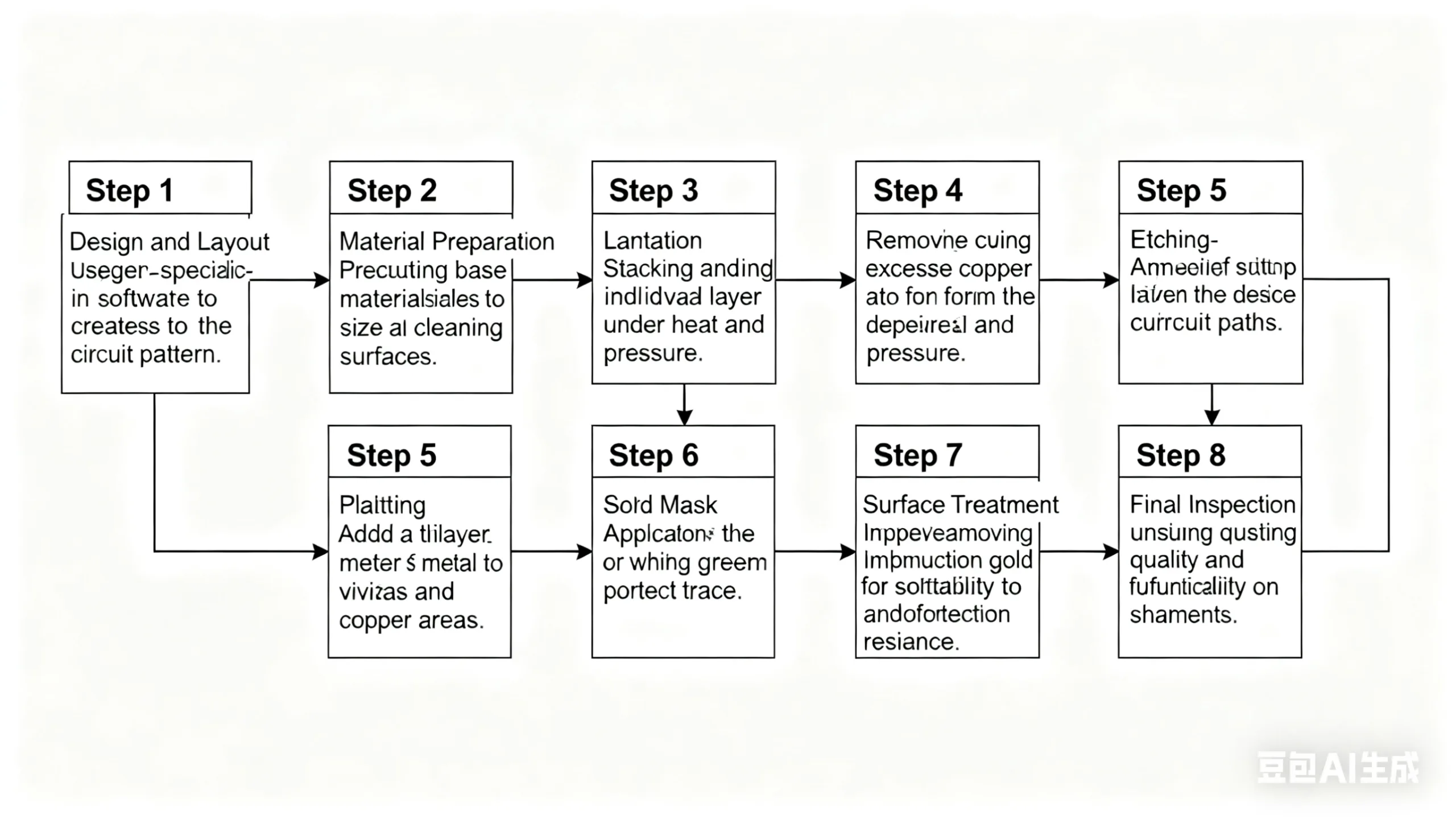
The manufacturing process of a 10-layer ENIG board involves several steps:
- การออกแบบและเค้าโครง: การใช้ซอฟต์แวร์พิเศษเพื่อสร้างรูปแบบวงจร.
- การเตรียมวัสดุ: การตัดวัสดุฐานเป็นขนาดและพื้นผิวการทำความสะอาด.
- การเคลือบ: การซ้อนและเชื่อมแต่ละชั้นภายใต้ความร้อนและความดัน.
- การแกะสลัก: การลบทองแดงส่วนเกินเพื่อสร้างเส้นทางวงจรที่ต้องการ.
- การชุบ: การเพิ่มชั้นโลหะบาง ๆ ลงใน Vias และพื้นที่ทองแดงที่เปิดเผย.
- แอปพลิเคชันมาสก์ประสาน: Applying the green or white coating to protect traces.
- การรักษาพื้นผิว: Applying immersion gold for solderability and corrosion resistance.
- การตรวจสอบขั้นสุดท้าย: สร้างความมั่นใจในคุณภาพและการใช้งานก่อนการจัดส่ง.
ใช้เคส
Common scenarios where a 10-layer ENIG board might be employed include:
- High-density interconnect applications in aerospace and defense systems.
- ระบบการสื่อสารขั้นสูงที่ต้องการการสูญเสียสัญญาณต่ำ.
- เครื่องมือทางการแพทย์แบบพกพาที่ต้องการประสิทธิภาพที่เชื่อถือได้ในสภาพแวดล้อมที่รุนแรง.
- ยานยนต์อิเล็กทรอนิกส์ที่ต้องการความแข็งแกร่งและอายุยืน.
โดยสรุป, the 10-layer ENIG board represents a significant advancement in printed circuit board technology offering unparalleled complexity and performance for modern electronic applications Its design flexibility combined with superior signal integrity and durability makes it an essential component in the development of next-generation high-end electronics and beyond


