
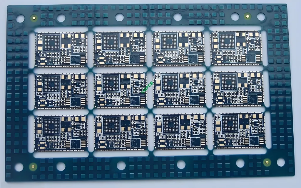
ภาพรวมของ PCB Bluetooth หลายชั้น 4 ชั้น
บลูทูธหลายชั้น 4 ชั้น พีซีบี เป็นผลิตภัณฑ์พิเศษที่ออกแบบมาเพื่อตอบสนองความต้องการที่เข้มงวดของแอปพลิเคชัน Bluetooth. PCB ประเภทนี้มีความสมบูรณ์ของสัญญาณสูง, เสถียรภาพทางความร้อน, และความน่าเชื่อถือ, ทำให้เป็นตัวเลือกที่เหมาะสำหรับอุปกรณ์ที่ใช้ Bluetooth ต่างๆ.

คำนิยาม
PCB Bluetooth หลายชั้น 4 ชั้นคือ แผงวงจรพิมพ์ ออกแบบมาโดยเฉพาะเพื่อรองรับการทำงานของโมดูล Bluetooth. ประกอบด้วยสื่อกระแสไฟฟ้าและฉนวนหลายชั้น วัสดุ, ให้เส้นทางไฟฟ้าที่ซับซ้อนและการเชื่อมต่อที่จำเป็นสำหรับการทำงานของอุปกรณ์ Bluetooth. คำว่า “4-ชั้น” หมายถึงจำนวนชั้นสื่อกระแสไฟฟ้า, ในขณะที่ “หลายชั้น” บ่งบอกว่ามีวัสดุนำไฟฟ้ามากกว่าสองชั้น.
ข้อกำหนดการออกแบบ
เมื่อออกแบบ PCB Bluetooth หลายชั้น 4 ชั้น, ต้องปฏิบัติตามข้อกำหนดที่สำคัญหลายประการ:
- คุณภาพวัสดุ: วัสดุ FR4 คุณภาพสูงเป็นสิ่งจำเป็นสำหรับความทนทานและเสถียรภาพทางความร้อน.
- การกำหนดค่าเลเยอร์: การออกแบบ 2 ชั้นเป็นมาตรฐาน, ช่วยให้สามารถกำหนดเส้นทางสัญญาณและพลังงานได้อย่างมีประสิทธิภาพ.
- ความหนาของทองแดง: ความหนาของทองแดง 1 ออนซ์ทำให้มั่นใจได้ว่าค่าการนำไฟฟ้าที่เพียงพอ.
- การรักษาพื้นผิว: การบำบัดพื้นผิวทองคำแบบแช่ช่วยเพิ่มการเชื่อมต่อและความต้านทานการกัดกร่อน.
- มิติติดตาม/อวกาศ: ขนาดการติดตามและพื้นที่ขั้นต่ำ 4mil (0.1มม) จำเป็นสำหรับรูปแบบวงจรที่แม่นยำ.
- คุณสมบัติพิเศษ: การออกแบบ PCB ครึ่งหลุมมักจะถูกรวมเข้าด้วยกันสำหรับการจัดวางส่วนประกอบเฉพาะและข้อกำหนดการบัดกรี.
หลักการทำงาน
PCB Bluetooth หลายชั้น 4 ชั้นทำงานตามหลักการของการนำไฟฟ้าและความสมบูรณ์ของสัญญาณ. ชั้นนำไฟฟ้าเป็นเส้นทางสำหรับสัญญาณไฟฟ้า, ในขณะที่เลเยอร์ฉนวนป้องกันการโต้ตอบที่ไม่พึงประสงค์ระหว่างสัญญาณเหล่านี้. การออกแบบแบบครึ่งรูช่วยให้กำหนดเส้นทางสัญญาณได้ดีขึ้นและลดการครอสทอล์ค. การรักษาพื้นผิวทองคำแบบแช่ให้การเชื่อมต่อที่ยอดเยี่ยมและป้องกันปัจจัยด้านสิ่งแวดล้อม.
การใช้งาน
PCB ประเภทนี้ส่วนใหญ่จะใช้ในอุปกรณ์ที่ใช้ Bluetooth, ซึ่งเป็นสิ่งสำคัญ ส่วนประกอบ ในระบบอิเล็กทรอนิกส์ต่างๆ เช่น อุปกรณ์สื่อสารไร้สาย, เครื่องเสียง, และไอโอที (อินเทอร์เน็ตของสรรพสิ่ง) อุปกรณ์. เหล่านี้รวมถึง:
- ลำโพงบลูทูธและหูฟัง
- คีย์บอร์ดและเมาส์ไร้สาย
- อุปกรณ์สมาร์ทโฮม
- เครื่องติดตามฟิตเนสและอุปกรณ์สวมใส่
- ระบบอัตโนมัติทางอุตสาหกรรม
การจำแนกประเภท
4-PCB Bluetooth หลายชั้นสามารถจำแนกตามคุณสมบัติเฉพาะและการใช้งานที่ต้องการ, เช่น:
- บอร์ดความสมบูรณ์ของสัญญาณ: เพื่อรักษาคุณภาพสัญญาณระดับสูงในการสื่อสาร Bluetooth.
- บอร์ดการจัดการความร้อน: เพื่อกระจายความร้อนที่เกิดจากส่วนประกอบ Bluetooth ได้อย่างมีประสิทธิภาพ.
- บอร์ดควบคุม: สำหรับจัดการและควบคุมฟังก์ชันต่างๆ ในระบบที่ใช้ Bluetooth.
วัสดุ
วัสดุหลักที่ใช้ในการก่อสร้าง PCB Bluetooth หลายชั้น 4 ชั้น ได้แก่:
- วัสดุฐาน: FR4, วัสดุไฟเบอร์กลาสที่ทนไฟที่รู้จักกันในคุณสมบัติไดอิเล็กตริกที่ยอดเยี่ยมและความแข็งแรงเชิงกลของมัน.
- วัสดุนำไฟฟ้า: ทองแดง, ใช้สำหรับร่องรอยนำไฟฟ้า.
- การรักษาพื้นผิว: ทองแช่, ซึ่งช่วยเพิ่มการเชื่อมต่อและให้ความต้านทานการกัดกร่อน.
ผลงาน
ประสิทธิภาพของ PCB Bluetooth หลายชั้น 4 ชั้นมีลักษณะเฉพาะคือ:
- ความสมบูรณ์ของสัญญาณสูง: เนื่องจากขนาดร่องรอยและพื้นที่ที่แม่นยำและการออกแบบครึ่งรู.
- เพิ่มเสถียรภาพทางความร้อน: วัสดุฐาน FR4 ช่วยกระจายความร้อนได้อย่างมีประสิทธิภาพยิ่งขึ้น.
- การเชื่อมต่อที่เชื่อถือได้: มั่นใจได้จากการรักษาพื้นผิวทองคำ.
- ความทน: ปรับปรุงโดยวัสดุฐาน FR4 ที่แข็งแกร่ง.
- ประสิทธิภาพทางไฟฟ้า: การสูญเสียสัญญาณและสัญญาณรบกวนน้อยที่สุดเนื่องจากการกำหนดค่าเลเยอร์ที่เหมาะสมที่สุด.
โครงสร้าง
โครงสร้างของ PCB Bluetooth หลายชั้น 4 ชั้นประกอบด้วย:
- วัสดุนำไฟฟ้าสองชั้น: สลับกับเลเยอร์ฉนวน.
- การบำบัดพื้นผิวทองคำ: สำหรับการเชื่อมต่อและการป้องกันที่เพิ่มขึ้น.
- การออกแบบครึ่งหลุม: สำหรับการจัดวางส่วนประกอบและข้อกำหนดการบัดกรีเฉพาะ.
คุณสมบัติ
คุณสมบัติที่สำคัญของ PCB Bluetooth หลายชั้น 4 ชั้นประกอบด้วย:
- การกำหนดค่าเลเยอร์ขั้นสูง: 4-การออกแบบเลเยอร์เพื่อการกำหนดเส้นทางสัญญาณที่เหนือกว่า.
- ความแม่นยำสูง: ด้วยขนาดการติดตามและพื้นที่ขั้นต่ำ 4mil (0.1มม).
- ตัวเลือกสีที่ปรับแต่งได้: มีสีดำหรือสีขาว.
- ความหนามาตรฐาน: ด้วยความหนาสำเร็จรูป 1.0 มม..
กระบวนการผลิต
กระบวนการผลิต PCB Bluetooth หลายชั้น 4 ชั้นเกี่ยวข้องกับหลายขั้นตอน:
- การเตรียมวัสดุ: การเลือกและเตรียมแผ่น FR4 และฟอยล์ทองแดง.
- การซ้อนชั้น: การรวมชั้นทองแดงและฉนวนเข้าด้วยกัน.
- การแกะสลัก: การลบทองแดงส่วนเกินเพื่อสร้างรูปแบบวงจรที่ต้องการ.
- การชุบ: การใช้การรักษาพื้นผิวทองคำแบบแช่.
- การเคลือบ: การรวมเลเยอร์ภายใต้ความร้อนและความดัน.
- การขุดเจาะ: การสร้างหลุมสำหรับส่วนประกอบและ vias ผ่านหลุม.
- แอปพลิเคชันมาสก์ประสาน: ปกป้องวงจรจากสะพานประสานและปัจจัยด้านสิ่งแวดล้อม.
- การพิมพ์ซิลค์สกรีน: การเพิ่มข้อความและสัญลักษณ์สำหรับการจัดวางส่วนประกอบและการระบุตัวตน.
- การควบคุมคุณภาพ: ทำให้มั่นใจว่า PCB เป็นไปตามข้อกำหนดและมาตรฐานการออกแบบทั้งหมด.
ใช้สถานการณ์
PCB Bluetooth หลายชั้น 4 ชั้นเหมาะอย่างยิ่งสำหรับสถานการณ์ที่:
- ความสมบูรณ์ของสัญญาณสูงเป็นสิ่งสำคัญ.
- จำเป็นต้องมีการเชื่อมต่อที่เชื่อถือได้และทนทาน.
- การจัดการระบายความร้อนที่มีประสิทธิภาพเป็นสิ่งจำเป็นเพื่อรักษาอุณหภูมิในการทำงานให้คงที่.
- การรักษาพื้นผิวขั้นสูงเป็นสิ่งจำเป็นสำหรับประสิทธิภาพที่เพิ่มขึ้น.


