

รู้เบื้องต้นเกี่ยวกับ 6 เลเยอร์ PCB
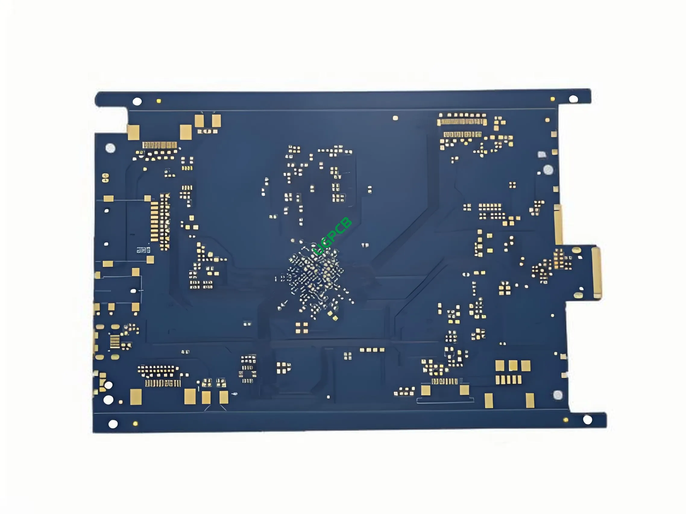
ที่ 6 Layer PCB is a sophisticated electronic component designed for high-performance applications requiring complex circuitry. It consists of six layers of conductive material, โดยทั่วไปแล้วทองแดง, คั่นด้วยเลเยอร์ฉนวน. This multilayer structure allows for greater functionality and compactness compared to single or double-sided PCBs.
ก 6 เลเยอร์ PCB?
อัน 6 เลเยอร์ PCB, หรือ แผงวงจรพิมพ์, is an advanced electronic substrate that features six layers of conductive pathways embedded within insulating layers. These layers are meticulously arranged to create intricate circuit designs suitable for demanding electronic applications. The additional layers provide enhanced signal integrity, การกระจายพลังงาน, and thermal management capabilities.
ข้อกำหนดการออกแบบ
Designing a 6 Layer PCB involves several critical considerations:
- การเลือกวัสดุ: Common materials include S1141, S1000, และ 370ชั่วโมง, chosen based on their electrical properties and compatibility with the manufacturing process.
- เลเยอร์ stackup: Determines the arrangement of signal and ground planes, crucial for minimizing crosstalk and ensuring reliable signal transmission.
- ความหนาของทองแดง: Typically specified as 1/H/H/H/H1 OZ, indicating varying thicknesses across different layers to optimize performance and cost.
- การรักษาพื้นผิว: Options like Immersion Gold or OSP (Organo-Silicon Protection) are applied to protect the copper surfaces and enhance solderability.
มันทำงานอย่างไร?
ที่ 6 Layer PCB functions by providing a platform for electrical components to be interconnected through a series of conductive paths etched onto its surface. Each layer contains specific patterns of copper traces that form circuits when connected via plated through-holes or vias. The multiple layers enable more complex circuit designs without increasing the board’s footprint, making it ideal for modern electronic devices where space is limited.
การใช้งาน
Due to their complexity and capability to handle high-speed signals with minimal interference, 6 Layer PCBs are widely used in consumer electronics such as smartphones, แท็บเล็ต, แล็ปท็อป, และอุปกรณ์พกพาอื่นๆ. They are also found in automotive electronics, อุปกรณ์การแพทย์, and industrial controls where reliability and performance are paramount.

การจำแนกประเภท
6 Layer PCBs can be classified based on several factors:
- โดยวัสดุ: As mentioned, they may use S1141, S1000, or 370HR depending on the required characteristics.
- โดยการสมัคร: General-purpose or specialized for specific industries like telecommunications, การบินและอวกาศ, or defense.
- โดยการรักษาพื้นผิว: Different finishes like Immersion Gold or OSP cater to various environmental conditions and soldering processes.
วัสดุที่ใช้
The primary materials used in manufacturing 6 Layer PCBs include:
- วัสดุฐาน: Often fiberglass-reinforced epoxy resins (FR-4), which offer excellent mechanical strength and thermal stability.
- ฟอยล์ทองแดง: Varying thicknesses are used to balance conductivity and cost-effectiveness.
- หน้ากากบัดกรี: Typically green in color, ช่วยปกป้องร่องรอยทองแดงจากการออกซิเดชั่นและการลัดวงจรโดยไม่ตั้งใจ.
- Silk Screen: A white coating used for labeling components and providing instructions for assembly.
ลักษณะประสิทธิภาพ
Key performance attributes of a 6 Layer PCB include:
- ความสมบูรณ์ของสัญญาณ: Enhanced by strategic layer placement and grounding schemes.
- การจัดการความร้อน: Improved heat dissipation due to larger copper areas and potentially thicker boards.
- ความแข็งแรงเชิงกล: Multilayer construction adds rigidity, reducing the risk of damage during handling or operation.
องค์ประกอบเชิงโครงสร้าง
ตามโครงสร้าง, อัน 6 Layer PCB comprises:
- ชั้นนำไฟฟ้า: Six layers of copper traces separated by dielectric materials.
- เลเยอร์ฉนวน: ป้องกันกางเกงขาสั้นไฟฟ้าระหว่างชั้นนำไฟฟ้า.
- สิ่งของต่าง ๆ: Conductive holes that connect different layers, allowing vertical integration of circuits.
คุณสมบัติที่โดดเด่น
Some notable features of a 6 Layer PCB are:
- ความหนาแน่นสูง: Allows for complex circuit designs within a compact form factor.
- ความน่าเชื่อถือ: Multilayer design improves resistance to electromagnetic interference (อีเอ็มไอ).
- ความอเนกประสงค์: Suitable for a wide range of applications due to customizable layer configurations and material choices.
กระบวนการผลิต
The manufacturing process of a 6 Layer PCB involves several steps:
- การออกแบบและเค้าโครง: การใช้ซอฟต์แวร์พิเศษเพื่อสร้างรูปแบบวงจร.
- การเตรียมวัสดุ: การตัดวัสดุฐานเป็นขนาดและพื้นผิวการทำความสะอาด.
- การเคลือบ: การซ้อนและเชื่อมแต่ละชั้นภายใต้ความร้อนและความดัน.
- การแกะสลัก: การลบทองแดงส่วนเกินเพื่อสร้างเส้นทางวงจรที่ต้องการ.
- การชุบ: การเพิ่มชั้นโลหะบาง ๆ ลงใน Vias และพื้นที่ทองแดงที่เปิดเผย.
- แอปพลิเคชันมาสก์ประสาน: Applying the green coating to protect traces.
- Silk Screen Printing: Adding text and symbols for component placement.
- การตรวจสอบขั้นสุดท้าย: สร้างความมั่นใจในคุณภาพและการใช้งานก่อนการจัดส่ง.
ใช้เคส
Common scenarios where a 6 Layer PCB might be employed include:
- แอพพลิเคชั่นเชื่อมต่อระหว่างกันที่มีความหนาแน่นสูงในอุปกรณ์มือถือ.
- ระบบการสื่อสารขั้นสูงที่ต้องการการสูญเสียสัญญาณต่ำ.
- เครื่องมือทางการแพทย์แบบพกพาที่ต้องการประสิทธิภาพที่เชื่อถือได้ในสภาพแวดล้อมที่รุนแรง.
- ยานยนต์อิเล็กทรอนิกส์ที่ต้องการความแข็งแกร่งและอายุยืน.
โดยสรุป, ที่ 6 Layer PCB represents a significant advancement in printed circuit board technology, นำเสนอความซับซ้อนและประสิทธิภาพที่เหนือชั้นสำหรับการใช้งานอิเล็กทรอนิกส์ที่ทันสมัย. Its design flexibility, combined with superior signal integrity and durability, makes it an essential component in the development of next-generation consumer electronics and beyond.


