
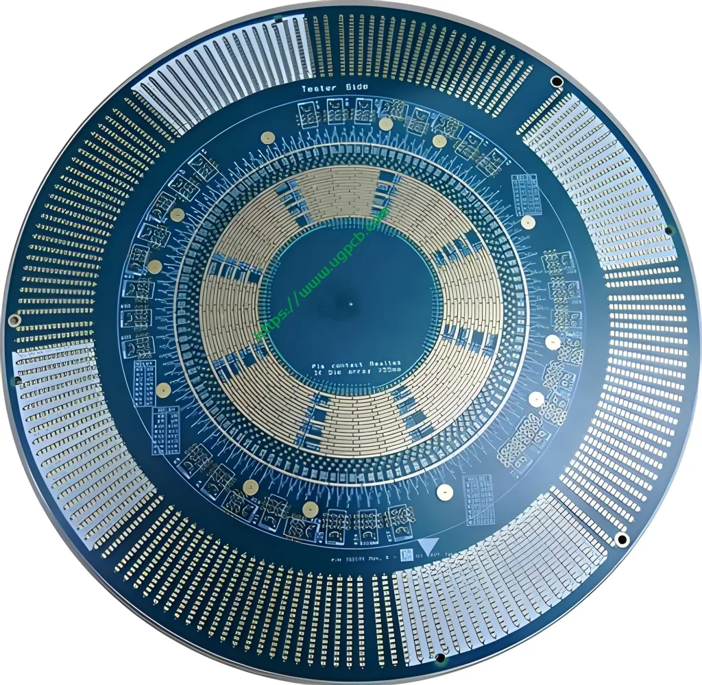
ATE Test Chip PCB Overview
The ATE test chip PCB is a specialized แผงวงจรพิมพ์ designed for use in automated test equipment (กิน) systems for testing semiconductor chips. นี้ พีซีบี plays a crucial role in ensuring the quality and reliability of chips before they are integrated into electronic devices. Below is a detailed introduction to the ATE test chip PCB, ครอบคลุมข้อมูลทั่วไป, การจำแนกประเภท, วัสดุ, ผลงาน, โครงสร้าง, คุณสมบัติ, กระบวนการผลิต, และสถานการณ์การใช้งาน.
การจำแนกประเภท
ATE test chip PCBs are classified based on their layer count, material composition, และข้อกำหนดการใช้งานเฉพาะ. รุ่นที่นำเสนอที่นี่, ATE test chip PCB, is a 12-layer PCB, indicating its complexity and ability to handle intricate testing scenarios.
องค์ประกอบของวัสดุ
The ATE test chip PCB is constructed using isola 370hr material, a high-performance, high-reliability substrate known for its excellent electrical and thermal properties. This material ensures the PCB’s ability to withstand the demanding test conditions and provide stable performance.
ลักษณะประสิทธิภาพ
The ATE test chip PCB excels in several performance areas, รวมถึงความสามารถในการรองรับกระแสไฟฟ้าที่สูง, การสูญเสียสัญญาณต่ำ, และการจัดการระบายความร้อนที่ดีเยี่ยม. The use of 2OZ copper thickness for inner layers and 1OZ for outer layers enhances its electrical conductivity and thermal dissipation capabilities. นอกจากนี้, the immersion gold (5คุณ) surface finish provides superior corrosion resistance and solderability, ensuring reliable connections during testing.
การออกแบบโครงสร้าง
ตามโครงสร้าง, the ATE test chip PCB features a board thickness of 3.0mm, providing a robust foundation for the complex circuitry and ส่วนประกอบ. The green color not only adds a visual distinction but also aids in inspection and troubleshooting processes.
คุณสมบัติที่โดดเด่น
The ATE test chip PCB stands out with its unique features, including its high layer count, advanced material composition, and immersion gold surface finish. คุณสมบัติเหล่านี้, combined with its precise design and manufacturing processes, make it an ideal choice for ATE chip testing applications.
กระบวนการผลิต
The production of ATE test chip PCBs involves a series of sophisticated steps:
- การเตรียมวัสดุ: The isola 370hr substrate is prepared and cut to the required dimensions.
- การเคลือบทองแดง: ฟอยล์ทองแดงถูกเคลือบไว้กับพื้นผิว, with specific attention to the inner layer 2OZ and outer layer 1OZ thickness requirements.
- รูปแบบวงจร: รูปแบบวงจรที่ต้องการจะถูกแกะสลักลงบนฟอยล์ทองแดงโดยใช้เทคนิคการแกะสลักที่มีความแม่นยำ.
- การซ้อนชั้นและการเคลือบ: ซ้อนกันหลายชั้นและเคลือบเข้าด้วยกัน, รับประกันการจัดตำแหน่งและการยึดเกาะที่แม่นยำ.
- การเจาะและการชุบ: Holes are drilled for component mounting and interconnection, and then plated to enhance conductivity.
- การประยุกต์ใช้การตกแต่งพื้นผิว: The immersion gold (5คุณ) coating is applied to provide corrosion resistance and solderability.
- การตรวจสอบและทดสอบขั้นสุดท้าย: PCB ผ่านการตรวจสอบและทดสอบอย่างเข้มงวดเพื่อให้มั่นใจว่าเป็นไปตามข้อกำหนดและข้อกำหนดด้านประสิทธิภาพ.
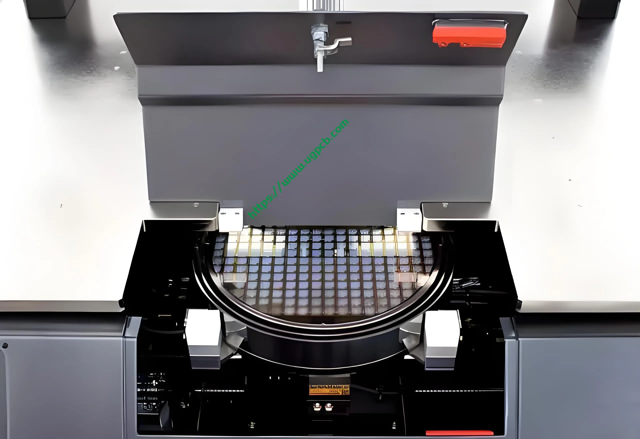
สถานการณ์การใช้งาน
ATE test chip PCBs are primarily used in automated test equipment systems for the testing and validation of semiconductor chips. พวกมันมีความสำคัญในอุตสาหกรรมเซมิคอนดักเตอร์, where high-reliability testing is crucial for ensuring the quality and performance of chips before they are integrated into electronic devices. By utilizing ATE test chip PCBs, manufacturers can quickly and accurately identify any defects or issues in the chips, ensuring that only high-quality products are shipped to customers.


