
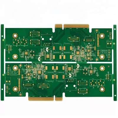
Overview of 6 Layer Golden Finger PCB
ที่ 6 Layer Golden Finger PCB is a high-precision, multi-layered printed circuit board designed for advanced electronic applications. This product combines multiple layers of conductive traces and insulating materials to provide exceptional performance and reliability in various electronic devices.
คำนิยาม
อัน 6 Layer Golden Finger PCB is a type of multi-layer printed circuit board (พีซีบี) that features six individual layers of conductive material, คั่นด้วยเลเยอร์ฉนวน. คำว่า “Golden Finger” refers to the specific surface treatment applied to the edges of the board, which involves immersion gold and additional gold plating on the contact fingers.
ข้อกำหนดการออกแบบ
When designing a 6 Layer Golden Finger PCB, several key requirements must be considered:
- คุณภาพวัสดุ: High-quality FR4 material is essential for durability and performance.
- การกำหนดค่าเลเยอร์: Six layers are needed to accommodate complex circuitry and signal routing.
- ความหนาของทองแดง: A standard copper thickness of 1OZ ensures adequate conductivity.
- การรักษาพื้นผิว: Immersion gold with additional gold finger plating enhances connectivity and corrosion resistance.
- มิติติดตาม/อวกาศ: A minimum trace/space of 4mil/4mil is required for precise circuit patterns.
- กระบวนการพิเศษ: The gold finger process with a thickness of 0.1um is critical for reliable edge connections.
หลักการทำงาน
ที่ 6 Layer Golden Finger PCB operates based on the principles of electrical conductivity and insulation. Conductive traces on different layers create pathways for electrical signals, ในขณะที่เลเยอร์ฉนวนป้องกันการโต้ตอบที่ไม่พึงประสงค์ระหว่างสัญญาณเหล่านี้. The gold finger edges facilitate easy insertion into connectors, ensuring stable and reliable connections.
การใช้งาน
This type of PCB is widely used in applications that require high precision and reliability, เช่น:
- High-speed digital circuits
- Telecommunications equipment
- Advanced computing systems
- อุปกรณ์อิเล็กทรอนิกส์ยานยนต์
- อุปกรณ์การแพทย์
การจำแนกประเภท
6 Layer Golden Finger PCBs can be classified based on their intended use, เช่น:
- Signal Processing Boards: For handling high-frequency signals in communication devices.
- บอร์ดการกระจายพลังงาน: เพื่อจัดการแหล่งจ่ายไฟในระบบอิเล็กทรอนิกส์ที่ซับซ้อน.
- บอร์ดควบคุม: For controlling and managing various functions in electronic devices.
วัสดุ
วัสดุหลักที่ใช้ในการก่อสร้างก 6 Layer Golden Finger PCB include:
- วัสดุฐาน: FR4, วัสดุไฟเบอร์กลาสที่ทนไฟที่รู้จักกันในคุณสมบัติไดอิเล็กตริกที่ยอดเยี่ยมและความแข็งแรงเชิงกลของมัน.
- วัสดุนำไฟฟ้า: ทองแดง, ใช้สำหรับร่องรอยนำไฟฟ้า.
- การรักษาพื้นผิว: Immersion gold and additional gold plating for the gold fingers.
ผลงาน
The performance of a 6 Layer Golden Finger PCB is characterized by:
- ความสมบูรณ์ของสัญญาณสูง: เนื่องจากขนาดการติดตาม/อวกาศที่แม่นยำและวัสดุคุณภาพ.
- การเชื่อมต่อที่เชื่อถือได้: Ensured by the gold finger surface treatment.
- ความทน: Enhanced by the robust FR4 base material and immersion gold finish.
- ประสิทธิภาพทางไฟฟ้า: การสูญเสียสัญญาณและสัญญาณรบกวนน้อยที่สุดเนื่องจากการกำหนดค่าเลเยอร์ที่เหมาะสมที่สุด.
โครงสร้าง
โครงสร้างของก 6 Layer Golden Finger PCB consists of:
- วัสดุนำไฟฟ้าหกชั้น: สลับกับเลเยอร์ฉนวน.
- Gold Finger Edges: Plated with a thin layer of gold for enhanced connectivity.
- Protective Layers: Including solder mask and silkscreen for protection and identification.
คุณสมบัติ
Key features of the 6 Layer Golden Finger PCB include:
- การรักษาพื้นผิวขั้นสูง: Immersion gold plus gold finger for superior connection quality.
- ความแม่นยำสูง: With a minimum trace/space of 4mil/4mil.
- ตัวเลือกสีที่ปรับแต่งได้: มีให้บริการในสีเขียวหรือสีขาว.
- ความหนามาตรฐาน: With a finished thickness of 1.6mm.
กระบวนการผลิต
The production process for a 6 Layer Golden Finger PCB involves several steps:
- การเตรียมวัสดุ: การเลือกและเตรียมแผ่น FR4 และฟอยล์ทองแดง.
- การซ้อนชั้น: ชั้นทองแดงและวัสดุฉนวนสลับกัน.
- การแกะสลัก: การลบทองแดงส่วนเกินเพื่อสร้างรูปแบบวงจรที่ต้องการ.
- การชุบ: Applying immersion gold and additional gold finger plating.
- การเคลือบ: การรวมเลเยอร์ภายใต้ความร้อนและความดัน.
- การขุดเจาะ: การสร้างหลุมสำหรับส่วนประกอบและ vias ผ่านหลุม.
- แอปพลิเคชันมาสก์ประสาน: ปกป้องวงจรจากสะพานประสานและปัจจัยด้านสิ่งแวดล้อม.
- การพิมพ์ซิลค์สกรีน: การเพิ่มข้อความและสัญลักษณ์สำหรับการจัดวางส่วนประกอบและการระบุตัวตน.
- การควบคุมคุณภาพ: ทำให้มั่นใจว่า PCB เป็นไปตามข้อกำหนดและมาตรฐานการออกแบบทั้งหมด.
ใช้สถานการณ์
ที่ 6 Layer Golden Finger PCB is ideal for scenarios where:
- ความสมบูรณ์ของสัญญาณสูงเป็นสิ่งสำคัญ.
- จำเป็นต้องมีการเชื่อมต่อที่เชื่อถือได้และทนทาน.
- ข้อ จำกัด ด้านพื้นที่จำเป็นต้องมีการออกแบบที่กะทัดรัดและมีประสิทธิภาพ.
- การรักษาพื้นผิวขั้นสูงเป็นสิ่งจำเป็นสำหรับประสิทธิภาพที่เพิ่มขึ้น.


