
Introduction to IC Chip Test PCB
Overview and Definition
An IC Chip Test PCB, or Integrated Circuit Chip Test แผงวงจรพิมพ์, is a specialized circuit board designed for testing integrated circuit chips. It ensures that the chips meet the required specifications before they are used in electronic devices.
หลักการทำงาน
The IC Chip Test PCB works by connecting the integrated circuit chip to various test points on the พีซีบี. These test points measure the electrical characteristics of the chip, such as voltage, ปัจจุบัน, and resistance, to verify its functionality.
การใช้งาน
IC Chip Test PCBs are used in the manufacturing and quality control processes of electronic devices. They are essential for ensuring that only functioning and reliable chips are used in the final products.

Types of IC Chip Test PCBs
There are different types of IC Chip Test PCBs based on their design and functionality:
- Functional Test PCBs: Used to test the overall functionality of the chip.
- Parameter Test PCBs: Used to measure specific parameters like power consumption, ความเร็ว, and temperature.
วัสดุและการก่อสร้าง
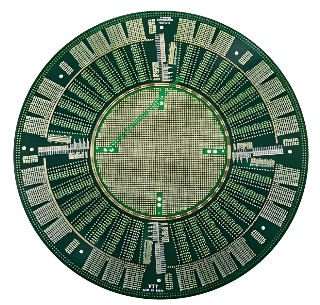
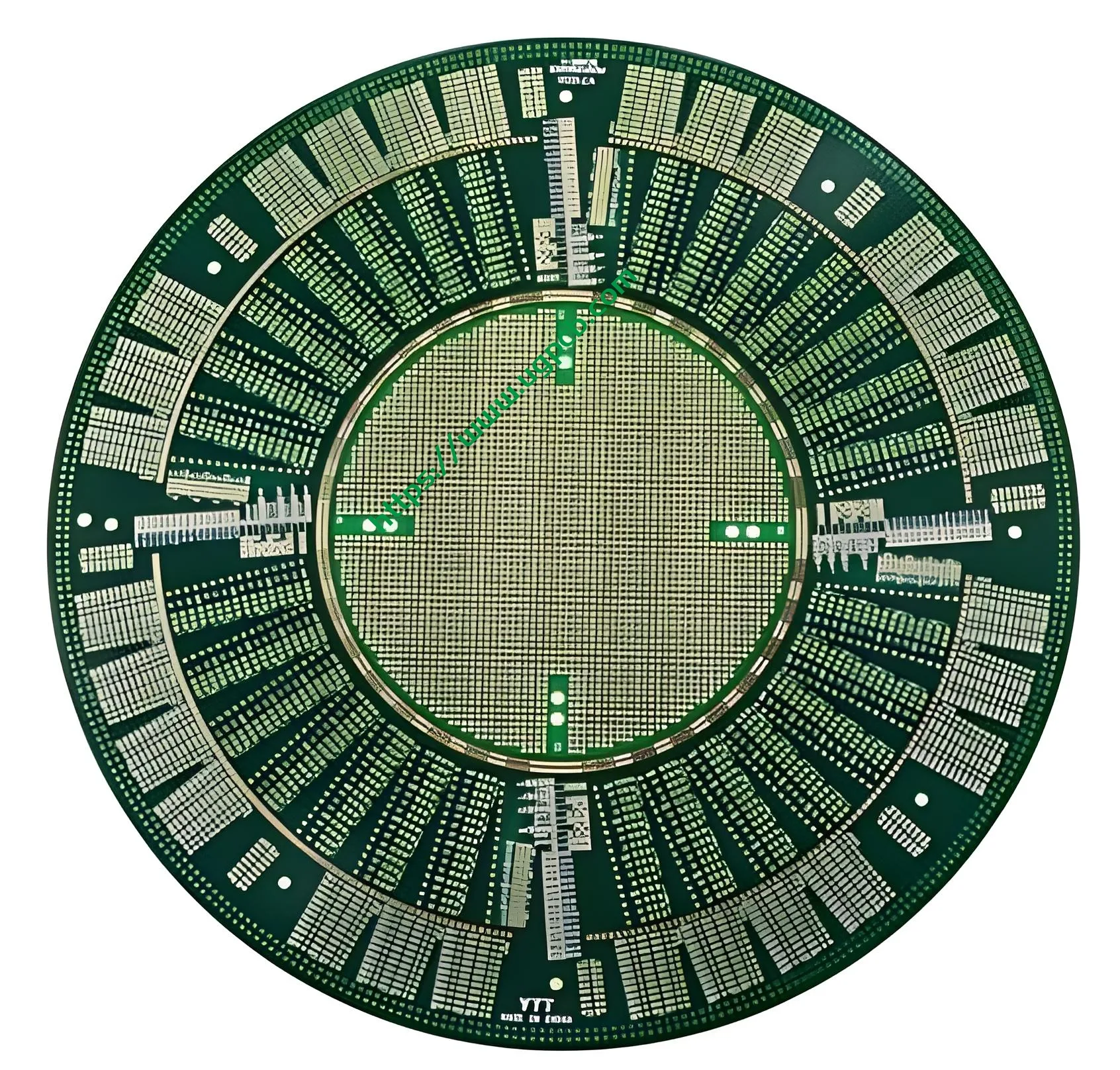
- วัสดุ: TU872SLS, วัสดุอีพ็อกซี่คุณภาพสูง.
- เลเยอร์: 20 ชั้น, ให้ความแข็งแกร่งและความสมบูรณ์ของสัญญาณที่ดีขึ้น.
- สี: มีให้บริการในสีเขียวหรือสีขาว.
- ความหนาสำเร็จรูป: 2.0มม, สร้างความมั่นใจในความทนทานในขณะที่ผอมเพรียว.
- ความหนาของทองแดง: 1ออนซ์, ซึ่งมีการนำไฟฟ้าที่ดี.
- การรักษาพื้นผิว: Immersion gold with a thickness of at least 3U”, เพิ่มความต้านทานการกัดกร่อนและความสามารถในการบัดกรี.
ลักษณะประสิทธิภาพ
IC Chip Test PCBs are designed to accurately test the performance of integrated circuit chips. They support high-speed data transfer and are built to withstand repeated usage over time. เสร็จสิ้นการแช่ทองคำ.
คุณสมบัติเชิงโครงสร้าง
The structure of an IC Chip Test PCB includes multiple layers of copper traces sandwiched between layers of substrate material. การออกแบบหลายชั้นนี้ช่วยในการจัดการการกระจายความร้อนและปรับปรุงประสิทธิภาพไฟฟ้า. PCB ถูกเคลือบด้วยชั้นป้องกันเพื่อป้องกันความเสียหายและให้แน่ใจว่าอายุการใช้งาน.
กระบวนการผลิต
The production of an IC Chip Test PCB involves several steps:
- ออกแบบ: การใช้ซอฟต์แวร์พิเศษเพื่อสร้างเค้าโครงวงจร.
- การแกะสลัก: การลบทองแดงส่วนเกินเพื่อสร้างรูปแบบที่ต้องการ.
- การเคลือบ: รวมหลายเลเยอร์เข้าด้วยกัน.
- การชุบ: การเพิ่มชั้นโลหะบาง ๆ เพื่อปรับปรุงการเชื่อมต่อ.
- การตรวจสอบ: สร้างความมั่นใจว่า PCB เป็นไปตามมาตรฐานคุณภาพ.
- การประกอบ: การติดตั้งส่วนประกอบลงบน PCB.
- การทดสอบ: การตรวจสอบฟังก์ชั่นและประสิทธิภาพ.

ใช้เคส
IC Chip Test PCBs are used in various applications including:
- อุปกรณ์อิเล็กทรอนิกส์สำหรับผู้บริโภค: โทรศัพท์มือถือ, แท็บเล็ต, สมาร์ทวอทช์.
- เกี่ยวกับยานยนต์: In-car systems for navigation and entertainment.
- อุปกรณ์การแพทย์: อุปกรณ์การแพทย์แบบพกพา.
- ระบบอัตโนมัติอุตสาหกรรม: Control systems for machinery and robotics.
สรุปแล้ว, IC Chip Test PCBs play a crucial role in the electronics manufacturing process by ensuring the reliability and functionality of integrated circuit chips. การยอมรับอย่างกว้างขวางของพวกเขาในอุตสาหกรรมต่าง ๆ เน้นความเก่งกาจและความสำคัญของอุปกรณ์อิเล็กทรอนิกส์ที่ทันสมัย.


