
نظرة عامة على المنتج: ما هي لوحة الركيزة HDI IC?
تعد لوحة الركيزة HDI IC أمرًا بالغ الأهمية, الراقية لوحة الدوائر المطبوعة تم تصميمها خصيصًا للتوصيل البيني لحزمة أشباه الموصلات. انها بمثابة الواجهة الأساسية, توفير التوصيل الكهربائي, توزيع الطاقة, والدعم الميكانيكي بين قالب السيليكون ذو النبرة الدقيقة واللوحة الأم القياسية ثنائي الفينيل متعدد الكلور. يوفر UGPCB موثوقية عالية, تصنيع الركيزة HDI IC المتقدمة, تلبية المتطلبات الصارمة للتطبيقات بدءًا من الإلكترونيات الاستهلاكية وحتى الحوسبة عالية الأداء.
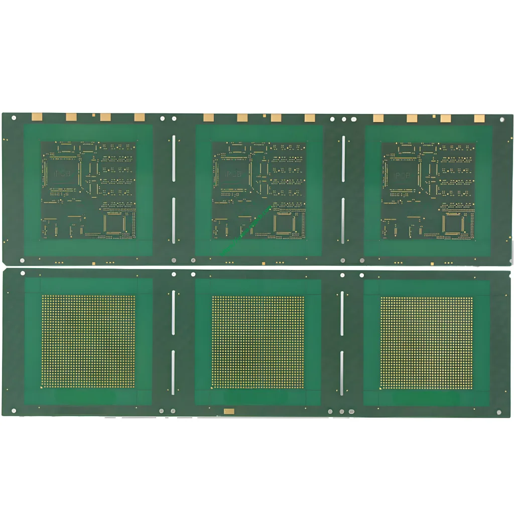
هذا المجلس, بنيت مع مادة SI10U في أ 6-طبقة (2+2+2) البناء وملف تعريف ضئيلة 0.6مم, يجسد أحدث ما توصلت إليه التكنولوجيا مؤشر التنمية البشرية تكنولوجيا. مع أ 35× 35 ملم حجم الوحدة, ويتميز أ 0.1ملم الحد الأدنى من الليزر عبر القطر, 30ميكرومتر الحد الأدنى لعرض التتبع / 70ميكرومتر الحد الأدنى للتباعد, و اينيبيك (النيكل غير الكهربائي البلاديوم الغمر الذهب) الانتهاء من السطح, مما يجعلها حلاً مثاليًا للتغليف عالي السرعة, عالية التردد, ورقائق متكاملة للغاية.
تحليل متعمق: تصميم, وظيفة, والتطبيقات
التعريف الأساسي & مبدأ العمل
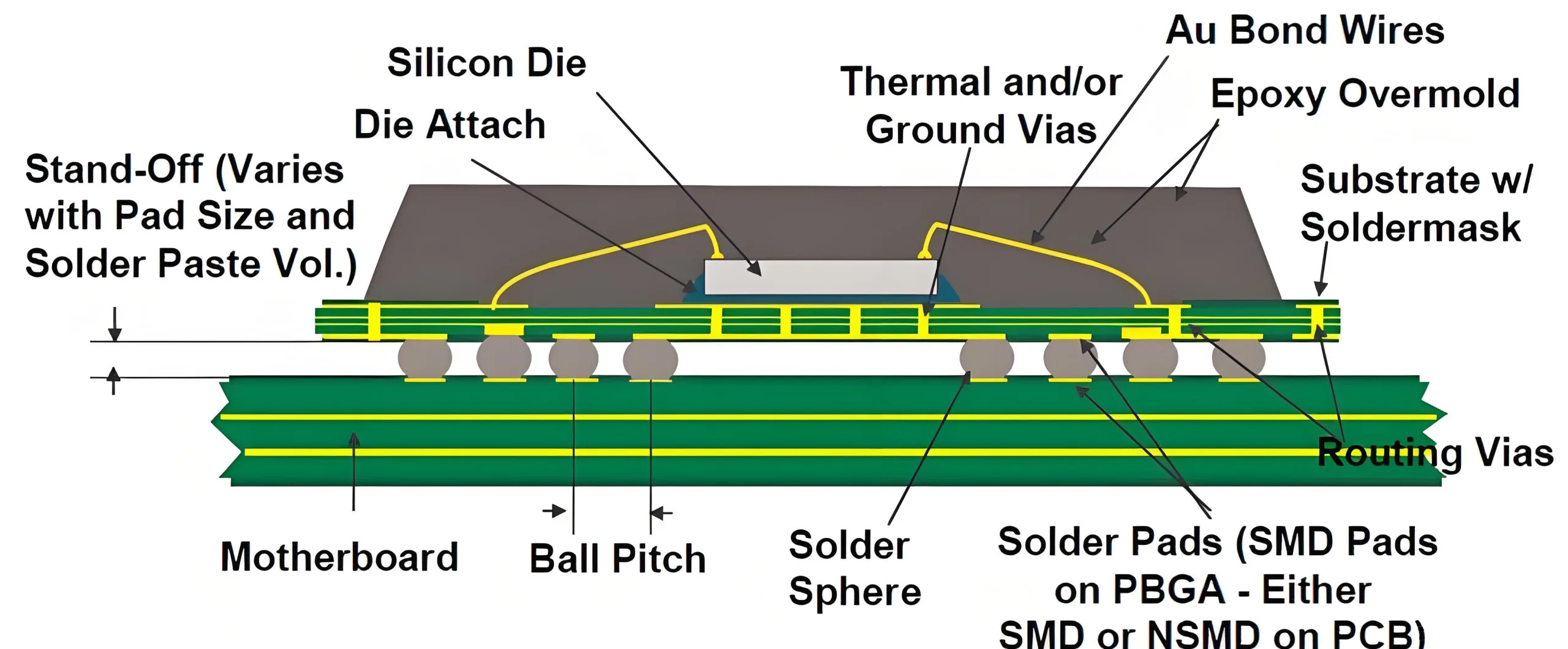
تم تصميم الركيزة IC HDI ل “مروحة خارج” مجموعة كثيفة من المطبات الدقيقة الناتجة عن قالب أشباه الموصلات, إعادة توزيع الاتصالات إلى درجة أكبر متوافقة مع المعيار تجميع ثنائي الفينيل متعدد الكلور عمليات مثل BGA (مصفوفة شبكة الكرة) تصاعد.
مبدأ العمل يتبع هذه السلسلة: يموت → Microbumps → HDI IC الركيزة (لإعادة توزيع الإشارة & الربط البيني) → كرات اللحام (بغا/CSP) → اللوحة الرئيسية ثنائي الفينيل متعدد الكلور. إنه محوري لسلامة الإشارة, تسليم الطاقة, والإدارة الحرارية.
اعتبارات التصميم الرئيسية
-
كومة المتابعة & السيطرة على المعاوقة: 6 طبقة (2+2+2) التراكم هو تصميم كلاسيكي لكثافة توجيه عالية. حساب المعاوقة الدقيق (عادة 50Ω أحادية الطرف أو 100Ω تفاضلية) أمر بالغ الأهمية لسلامة الإشارة.
-
مايكرو عبر الموثوقية: 0.1مم (100ميكرومتر) فيا صغيرة محفورة بالليزر هي المفتاح لكثافة الاتصال البيني. عبر الشكل, طلاء النحاس, ويجب تحسين عملية التعبئة لضمان موثوقية الدورة الحرارية.
-
تصنيع الخطوط الدقيقة: 30عرض التتبع ميكرومتر وتباعد 70 ميكرومتر هي المقاييس الأساسية لقدرة العملية, مما يؤثر بشكل مباشر على كثافة الإدخال/الإخراج والأداء الكهربائي.
-
الحرارية & الإدارة الميكانيكية: اختيار مادة SI10U يأخذ في الاعتبار معامل التمدد الحراري (CTE) مطابقة مع السيليكون لتقليل الضغط الحراري وتعزيز طول عمر المنتج.
المواد الأولية & خصائص الأداء
-
المواد الأساسية: SI10U. صفائح عالية الأداء توفر ثابت عازل منخفض (DK), عامل تبديد منخفض (ص), ارتفاع درجة حرارة التحول الزجاجي (تيراغرام), واستقرار الأبعاد ممتازة, مثالية للسرعة العالية, تطبيقات عالية التردد.
-
قناع اللحام: PSR-4000 AUS308. عالية الدقة, قناع لحام سائل قابل للتصوير عالي الموثوقية (إل بي إس إم) الذي يوفر تغطية دقيقة, عزل ممتاز, والمقاومة الكيميائية.
-
الانتهاء من السطح: اينيبيك. ترسب هذه النهاية طبقات متسلسلة من النيكل, البلاديوم, والذهب. يعمل النيكل كحاجز للانتشار, البلاديوم يمنع تآكل النيكل, وتوفر الطبقة الذهبية الرقيقة قابلية لحام فائقة وقدرة على ربط الأسلاك, مثالية للوسادات الدقيقة.
-
ملخص الأداء: كثافة عالية, سرعة عالية, موثوقية عالية, إدارة حرارية ممتازة, وسلامة الإشارة الفائقة.
تصنيف & سيناريوهات التطبيق
يتم تصنيف ركائز HDI IC حسب التكنولوجيا والتطبيق:
-
بواسطة التكنولوجيا: مع الأساسية (على سبيل المثال, هذا التراكم 6 لتر) أو أنواع عديمة النواة.
-
عن طريق التطبيق:
-
المعالجات المتقدمة: وحدة المعالجة المركزية, GPU, تتطلب رقائق تسريع الذكاء الاصطناعي الحد الأقصى من كثافة التوجيه وسرعة الإشارة.
-
متحرك & RF: معالجات تطبيقات الهواتف الذكية (ا ف ب) ووحدات الترددات اللاسلكية, حيث التصغير وملامح رقيقة (0.6مم) حرجة.
-
ذاكرة: ركائز الواجهة لذاكرة النطاق الترددي العالي (إتش بي إم).
-
الشبكات & السيارات: رقائق التبديل عالية السرعة ووحدات تحكم مجال ADAS.
-
عملية التصنيع في UGPCB & ضمان الجودة
يدمج إنتاج UGPCB العمليات الرائدة المتوافقة مع معايير IPC:
-
حفر الليزر: أنظمة الليزر فوق البنفسجية تخلق دقة 0.1ملم مايكرو فيا.
-
تصفيح & عبر ملء: يضمن الطلاء النبضي المتقدم اكتمال عملية التعبئة من أجل توصيلات موثوقة.
-
التصوير المتقدم: يتم تحقيق أنظمة التعرض المتطورة والأفلام الجافة عالية الدقة 30/70ميكرومتر تعريف الخط.
-
التصفيح: محاذاة دقيقة وضغط الطبقات الأساسية المتعددة والتحضير المسبق (ص).
-
التشطيب السطح: تطبيق اينيبيك طلاء من أجل قابلية اللحام المثالية.
-
اختبار شامل: يستخدم AOI (الفحص البصري الآلي), اختبار مسبار الطيران, واختبار المقاومة لضمان الامتثال.
ملكنا وقفة واحدة ثنائي الفينيل متعدد الكلور خدمة القدرة تمتد من الركيزة IC تصنيع إلى اللاحقة تجميع سمت و اختبار, تقديم حل التعبئة والتغليف الكامل.
لماذا تختار UGPCB لركيزة HDI IC الخاصة بك?
-
قدرة العملية المتقدمة: خبرة مثبتة في 30/70ميكرومتر أثر/مساحة و 0.1ملم مايكرو عبر تكنولوجيا.
-
خبره المواد: معرفة متعمقة بالمواد المتقدمة مثل SI10U للتوصية بالحلول الأمثل.
-
جودة لا هوادة فيها: صارمة, مراقبة الجودة على مستوى السيارات طوال العملية برمتها.
-
حل وقفة واحدة: نحن أكثر من أ صانع ثنائي الفينيل متعدد الكلور; نحن لك شريك PCBA, تقديم دعم التصميم, تصنيع, والتجمع.
-
دعم الخبراء: يوفر فريق هندسي متخصص سوق دبي المالي (تصميم للتصنيع) التحليل والاستشارة الفنية.
احصل على الحل المخصص لك الآن
سواء كنت تقوم بتطوير التالي منصة HPC, 5البنية التحتية G, أو نظام أداس, UGPCB المهنية تصنيع الركيزة HDI IC و خدمات تجميع PCBA هي أساسك للنجاح.
اتصل بنا اليوم للحصول على استشارة فنية مجانية وعرض أسعار! اسمح لخبرائنا بمساعدتك على تحسين أداء المنتج من خلال تحسينه تصميم الركيزة IC وموثوقة تصنيع ثنائي الفينيل متعدد الكلور العمليات.


