Breaking Limits: Inside UGPCB’s Cutting-Edge IC Substrate Design Capabilities
In an era of explosive AI computing power and 5G/6G bandwidth expansion, fingernail-sized chips now integrate billions of transistors. Todavía 60% of high-end chip failures stem not from silicon wafers themselves, but from defects in their critical carrier – the sustrato CI. This startling statistic underscores the extreme importance of substrate design.
Sustratos IC: The Invisible Foundation of Chip Performance
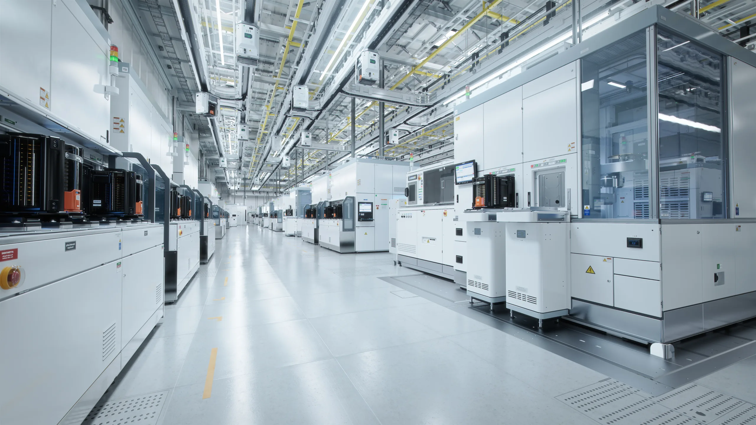
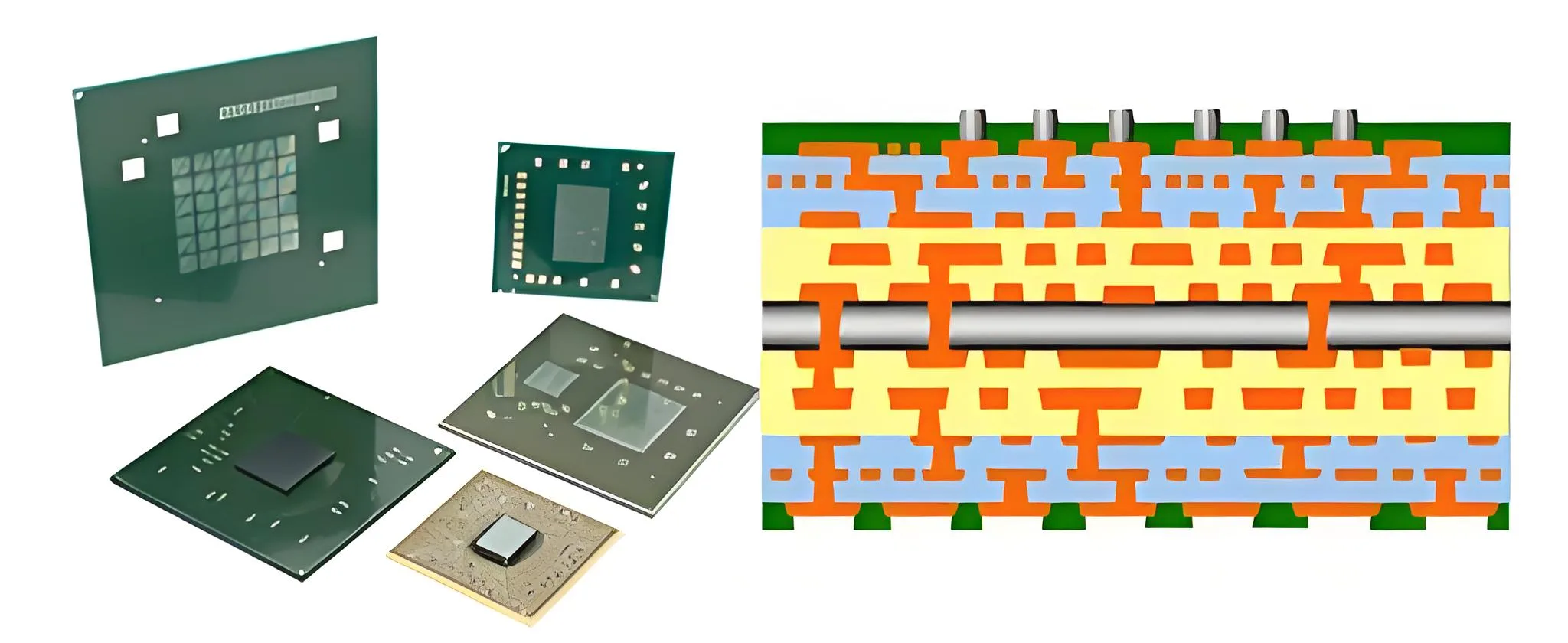
IC substrates are far more than simple connectors; they serve as the neural hub and power core between chips and the external world. With I/O counts surging to thousands (even 10,000+ for advanced GPUs/CPUs), trace widths/spacing shrinking below 15μm/15μm, and signal speeds exceeding 112Gbps, design precision now operates at nanometer scales. Thermal management failures and signal integrity degradation have become top killers in advanced packaging (2.5D/3D IC, Chiplet).
Key Formula: Impedance Control Accuracy (Z)
Z = (87 / √εr) × ln(5.98H / (0.8W + T))
Where εr = dielectric constant, H = dielectric thickness, W = trace width, T = copper thickness. UGPCB precisely controls these parameters to achieve ±5% impedance tolerance – surpassing the industry standard of ±10%.
Deconstructing UGPCB’s 5 Core IC Substrate Design Capabilities
1. Extreme High-Density Interconnect (IDH) Diseño
-
Microvia Mastery: Perforación láser (<50μm) and advanced plating enable any-layer HDI. Boosts routing channels by 40% in 0.2mm pitch BGA designs.
-
Ultra-Fine Line Breakthrough: Mass production of 12μm/12μm traces meets cutting-edge Chiplet requirements.
-
Advanced Stackups: Expertise in 16+ layer designs with hybrid materials (low-Dk/Df + high-Tg) for heterogeneous integration.
2. Nanoscale Signal/Power Integrity (SI/PI) Control
-
3D EM Simulation: Ansys HFSS and Cadence Sigrity eliminate reflections/crosstalk in 112G PAM4 channels.
-
PDN Optimization: Distributed decoupling networks reduce power supply noise (PSN) por 60%.
-
Loss Control: Ultra-low-profile copper (RTF/VLP) combined with impedance formula adherence minimizes insertion loss.
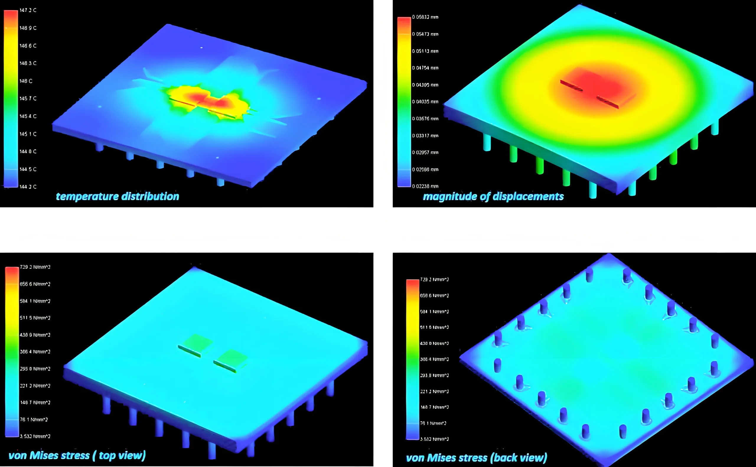
3. Thermal-Mechanical Reliability (TMV) Ingeniería
-
CTE Matching: Innovative materiales minimize warpage (<0.1%) by balancing chip (~2.6 ppm/°C) and substrate CTE (14-17 ppm/°C).
-
Multiphysics Simulation: COMSOL predicts solder joint fatigue during thermal cycling.
-
Thermal Architecture: Embedded heat pipes + >5 W/mK TIMs + optimized thermal vias boost system cooling.
4. Advanced Co-Design Packaging
-
Fab/OSAT Collaboration: Early DFM integration for FCBGA, WLP, and Si interposer processes.
-
Chiplet Expertise: UCIe-compliant high-bandwidth, low-latency interconnects.
-
Ciencia material: Strategic use of Ajinomoto ABF, MEGTRON series for RF/thermal/reliability needs.
5. DFM/DFT-Driven Design
-
Manufacturability Built-In: Design rules aligned with process capabilities maximize first-pass yield (FPY).
-
Testability Optimization: ATE-friendly test point layouts for complex substrates.
-
Design for Yield (DFY): Copper balancing and etch compensation improve production consistency.
UGPCB Success Story: Del diseño a la producción en masa
Caso: High-Power AI Accelerator FCBGA Substrate
-
Desafío: 45×45mm die, >800W power, 56Gbps PAM4 signals requiring extreme thermal/electrical performance.
-
Solución:
-
16-layer any-layer IDH with 12μm/12μm traces
-
TRONOME 7 centro (εr=3.3, Df=0.001) + precision impedance control
-
Embedded copper blocks + micro-via arrays (35% thermal resistance reduction)
-
Co-design with OSAT for bump/route optimization
-
-
Resultado: Passed SI/PI/thermal validation first-time, 98.5% producir, 6-month faster time-to-market.
Why Global Leaders Choose UGPCB as Their IC Substrate Partner
Con 100+ expert engineers, 300+ annual IC substrate designs, 20+ patents, and multimillion-dollar simulation labs, UGPCB entregas:
Key Differentiators
-
Liderazgo tecnológico: Defining next-gen substrate boundaries through R&D.
-
End-to-End Solutions: Design → Prototype → Volume production under one roof.
-
Manufacturing Certainty: In-house advanced fabs ensure design intent realization.
-
24/7 Responsiveness: Dedicated support teams with instant quotes.
Unlock Your Chip’s Full Potential Today!
Is your next-gen flagship chip limited by substrate bottlenecks? UGPCB’s experts are ready to provide:
✅ Free IC Substrate Design Feasibility Assessment
✅ Competitive PCBA Solution Quotes in 24 Hours
[Contact UGPCB’s IC Substrate Experts Now for Instant Support & Quote]
WeChat
Escanea el código QR con WeChat