SMT El rendimiento de impresión se dispara 60%! La ciencia detrás del diseño de plantillas de PCB de alta precisión & Selección
Esta lámina de acero inoxidable ultrafina es el sustento de la fabricación de productos electrónicos modernos: sus aberturas microscópicas dictan el destino de miles de millones de uniones de soldadura..
En líneas de montaje SMT, La impresión de pasta de soldadura contribuye a más 60% de defectos de proceso. Detrás de esta asombrosa estadística a menudo se esconde una herramienta crítica subestimada: la plantilla de PCB.
El papel fundamental de las plantillas en los procesos SMT
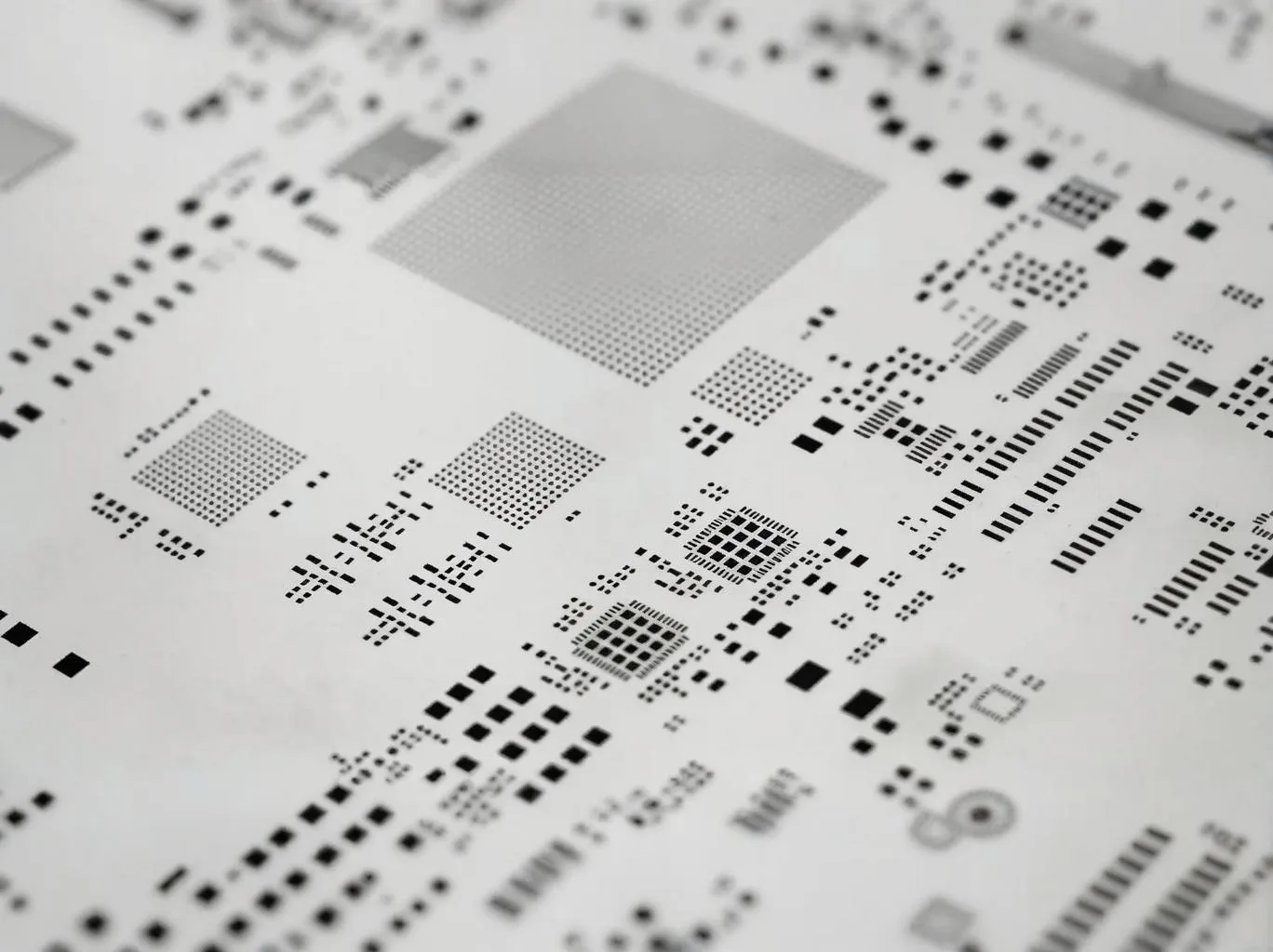
La plantilla es el molde de precisión de la fabricación electrónica moderna.. Su función principal es depositar dosis exactas de soldadura en pasta en los lugares designados. tarjeta de circuito impreso almohadillas. esta hoja, sólo 0,08-0,18 mm de espesor, Determina directamente la calidad y confiabilidad de las uniones soldadas..
A medida que se acelera la miniaturización de componentes, 0201 componentes (0.6×0,3 mm) y los BGA con paso de 0,35 mm se han convertido en algo habitual. Esto plantea graves desafíos para la tecnología de esténciles.: cuando los tamaños de apertura se reducen por debajo de 150 μm, las tasas de liberación de pasta caen en picado a menos de 70%.
Las plantillas de alta precisión deben cumplir tres métricas principales simultáneamente: estabilidad de tensión a 35-50N/cm², error de planitud de la superficie <0.1mm/m², y tolerancia posicional de apertura dentro de ±15μm (para componentes de paso fino por debajo de 0,4 mm). Estos parámetros impactan directamente en la precisión y consistencia de la impresión..
Elementos clave del diseño de plantilla de PCB de precisión
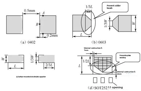
Diseño científico de parámetros geométricos.
Las relaciones de aspecto de apertura siguen la regla de oro IPC-7525: el rango óptimo es 1.5:1 a 2:1. Al procesar componentes QFP con paso de 0,5 mm, usando un 8-10mil (0.2-0.25milímetros) Una plantilla gruesa con diseños de apertura incremental puede aumentar la eficiencia de transferencia al 40%.
La proporción de área se correlaciona fuertemente con la eficiencia de transferencia (EL):
TE (%) = 100 × (Deposited Paste Volume / Aperture Volume)
El análisis estadístico muestra que con pasta fija y parámetros de impresión, 95% La variación de TE está determinada por la relación de área.. Las proporciones de área más altas producen desviaciones TE más pequeñas y una mejor repetibilidad del volumen de impresión..
Diseño estructural avanzado
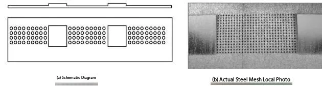
Abordar el hundimiento de la impresión de PCB flexible, UGPCB sistemas de soporte compuestos magnéticos desarrollados con adsorción al vacío por zonas, resolver completamente la deformación de las placas delgadas. Para sustratos de PTFE de alta frecuencia (p.ej., Material de Rogers), El posprocesamiento de grabado químico agregado elimina la pérdida de señal causada por las rebabas láser..
La tecnología de plantilla mejorada sobresale en escenarios de altura de componentes mixtos. Se deben seguir reglas de diseño críticas: Los bordes de los escalones deben mantener un espacio libre ≥ (1.0mm/1 mil)*altura del escalón desde los bordes de la abertura para evitar residuos de pasta.
Avances en los procesos de fabricación de plantillas
Tecnología de corte por láser
Las plantillas láser modernas utilizan láseres de fibra de precisión de 20 μm combinados con sistemas de visión CCD., logrando una precisión de rango completo <4μm. Las plataformas láser de UGPCB cuentan con compensación del punto focal en tiempo real, Garantizar la coherencia entre materiales: mantener una verticalidad de corte de 89 ± 1° incluso con materiales flexibles Kapton..
Innovación en nanorrevestimientos
Avances en el tratamiento de superficies: Recubrimientos antiadherentes compuestos a base de níquel triple vida útil de la plantilla, ampliando los ciclos de limpieza desde 800 a 5000+ huellas dactilares. Los recubrimientos modificados hidrofílicos para pastas a base de agua mejoran significativamente la liberación de soldadura sin plomo, reducir los residuos de pasta mediante 70%.
Aplicación de ciencia de materiales
UGPCB selecciona prima 301 acero inoxidable (límite elástico >550MPA, superando el estándar 304 210MPa del acero). Combinado con marcos de aleación de aluminio de grado aeroespacial (resistencia a la deformación >300tensión norte), La estabilidad estructural se mantiene incluso bajo impresión de alta velocidad..
Comparación de rendimiento de diferentes tipos de plantillas
| Parámetro | Plantilla láser | Plantilla grabada | Plantilla electroformada |
|---|---|---|---|
| Posicionamiento preciso. | ±15μm | ± 50 μm | ±8μm |
| mín.. Abertura | 40μm | 100μm | 30μm |
| Rugosidad de la pared (Real academia de bellas artes) | ≤0,8 μm | ≥1,5 μm | ≤0,5 μm |
| Plazo de ejecución de producción | 4 horas | 8 horas | 24 horas |
| Componentes adecuados | 01005 a BGA grande | ≥0603 | CSP de paso ultrafino |
| Rentabilidad | ★★★★ | ★★★ | ★★ |
Las plantillas láser dominan el mercado debido a su equilibrio precisión/coste, especialmente para la creación rápida de prototipos. UGPCB ofrece un tiempo de entrega de plantillas láser de 4 horas, compatible con Gerber X2, ODB++ y 15 otros formatos de diseño.
Cómo las propiedades de la plantilla afectan los defectos de impresión SMT
Las características de la plantilla influyen directamente en siete defectos principales de impresión SMT:
-
Desviación de espesor: Causa bolas de soldadura., puente, bermudas
-
Errores de recuento de apertura: Conduce a la tumba, desalineación
-
Tolerancia posicional: Resultados en puente, registro erróneo
-
Desviación de tamaño: Provoca soldadura excesiva/insuficiente
-
Defectos de forma: mala liberación, fijar
-
Rugosidad de la pared: Mayor residuo, liberación desigual
-
Limpieza insuficiente: Atasco, transferencia incompleta
Para 0201 componentes, UGPCB emplea aperturas trapezoidales de 30°-45° para suprimir la fijación. Para μBGA con paso de 0,3 mm, El nanopulido reduce la rugosidad de la pared a Ra<0.5μm, asegurando >92% liberación de pasta.
Uso de plantilla profesional & Soluciones de mantenimiento
Optimización del proceso de impresión
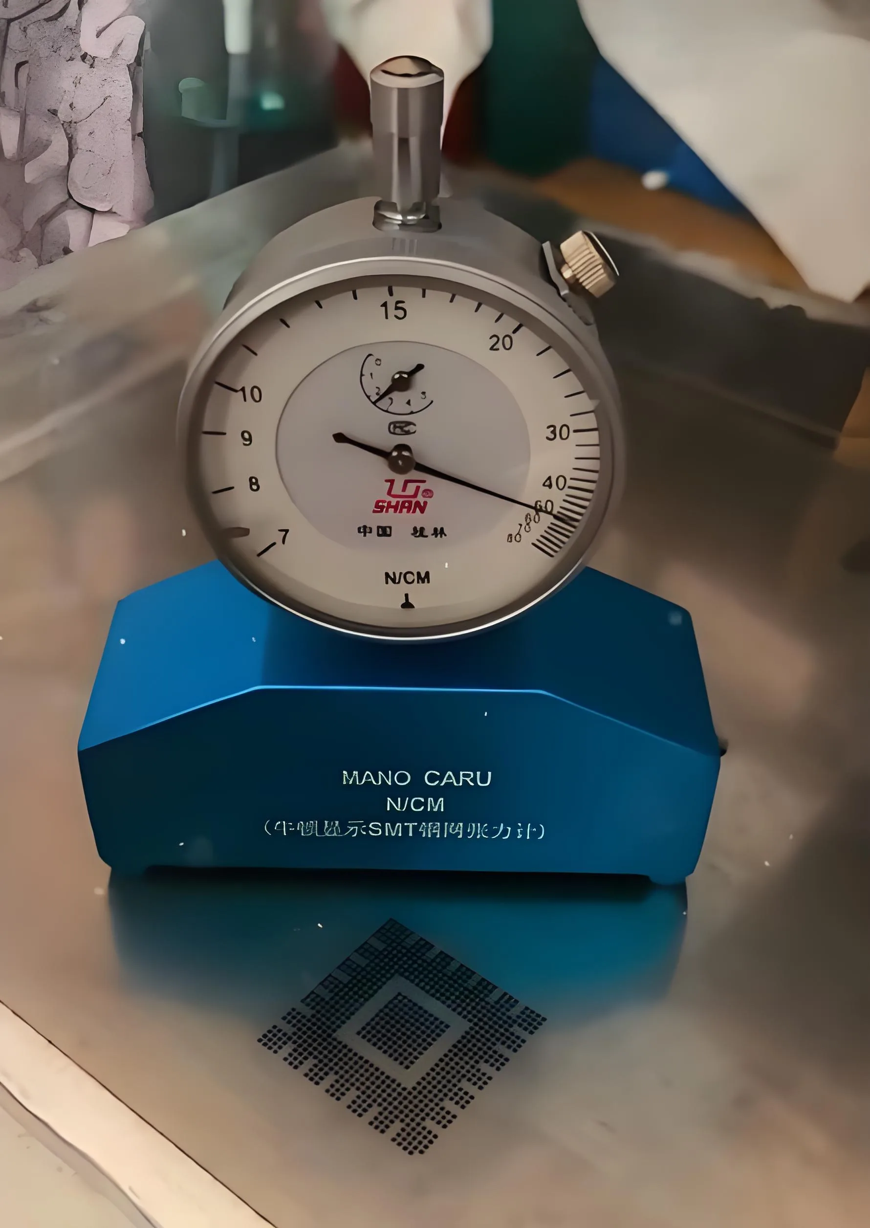
Los parámetros requieren ajuste dinámico: Presión de la escobilla de goma recomendada de 8,4 kgf/480 mm, velocidad de separación controlada a 1 mm/s. Para PCB de alta densidad, una técnica de separación de dos pasos (0.2mm/s para una separación inicial de 0,1 mm, luego liberación rápida) reduce significativamente los puentes.
Gestión completa del ciclo de vida
UGPCB proporciona un sistema de gemelo digital con seguimiento de chips RFID:
-
Conteo de impresiones
-
Curva de degradación de la tensión
-
Historial de limpieza
-
Correlaciones de calidad de impresión
Protocolo de mantenimiento profesional: Limpieza ultrasónica (disolvente de etanol) cada 50 huellas dactilares, controles de tensión mensuales, inspección trimestral de apertura óptica 3D.

Descripción general de las ventajas de la tecnología de plantilla UGPCB
Capacidades de fabricación de precisión
UGPCB opera centros láser multimillonarios equipados con:
-
Corte por láser asíncrono de doble cabezal
-
Inspección de luz blanca 3D en línea
-
Líneas automatizadas de nanorrecubrimiento
-
Salas blancas con control de temperatura/humedad
Habilitando 01005 plantillas de componentes (80× aperturas de 150 μm) con precisión posicional de ±12 μm: precisión líder en la industria.
Soporte de diseño inteligente
El sistema de optimización de apertura de IA identifica automáticamente los riesgos:
-
Alertas de conflicto de espaciado de componentes
-
Cálculo automático de la proporción de área
-
Simulación de tensión
-
Modelado de reología de pasta
Reciba informes de optimización dentro 10 minutos de carga de archivos, eliminando los costos de prueba y error.
Sistema de respuesta rápida
Red global de fabricación en la nube:
-
Centro de Asia: 4-hora de entrega
-
Centro de Europa: 8-hora de entrega
-
Centro de las Américas: 12-hora de entrega
Los servicios de emergencia las 8, 12 y 24 horas garantizan cero tiempos de inactividad en la línea de producción.
Nota crítica sobre el rendimiento de la plantilla
Cada disminución de 5 N/cm² en la tensión de la plantilla aumenta la probabilidad de registro incorrecto en 18%. Si se enfrenta al puente QFN, anulación BGA, o desecho de componentes en miniatura, Inspeccione el estado de su plantilla..
Los ingenieros de UGPCB dominan la sinergia entre el diseño de la plantilla y la reología de la soldadura en pasta. Ofrecemos soluciones personalizadas para pastas como SAC305 y SnBi57.. Póngase en contacto con nuestros consultores técnicos hoy para obtener su solución de plantilla optimizada y experimente la creación rápida de prototipos las 24 horas, lo que garantiza una deposición precisa de soldadura en pasta para un máximo rendimiento..
WeChat
Escanea el código QR con WeChat