
Introducción
The rapid advancement of Artificial Intelligence (AI), high-performance computing (HPC), and autonomous driving technologies is pushing data center routers and switches towards 800G and 1.6T interconnects. Como consecuencia, signal rates on PCB have surpassed 200 GBPS, entering the 224G era. This surge in data speed escalates system power consumption, causing temperatures on package substrates and PCBs to rise significantly, potentially exceeding 150°C in extreme scenarios. High-temperature environments substantially alter the Dielectric Constant (Dk) y factor de disipación (df) de Materiales de PCB, impacting transmission line impedance, insertion loss, and overall signal integrity (Y), thereby compressing system design margins. Based on IPC standards and authoritative experimental data, this article provides a deep dive into the effects of temperature on 224G PCB performance. It covers material properties, manufacturing processes, and signal integrity analysis, offering critical design insights for future 448G applications and Diseño de PCB de alta velocidad.
PCB Material Properties and Their Behavior at High Temperatures
PCB materials form the foundation of high-speed circuit design, primarily comprising dielectric substrates and metal conductors. For 224G and higher-rate applications, material selection directly determines signal attenuation, delay, y confiabilidad, making the choice of PCB laminate critical for successful tarjeta de circuito impreso desarrollo.
Key Parameters of Dielectric Materials
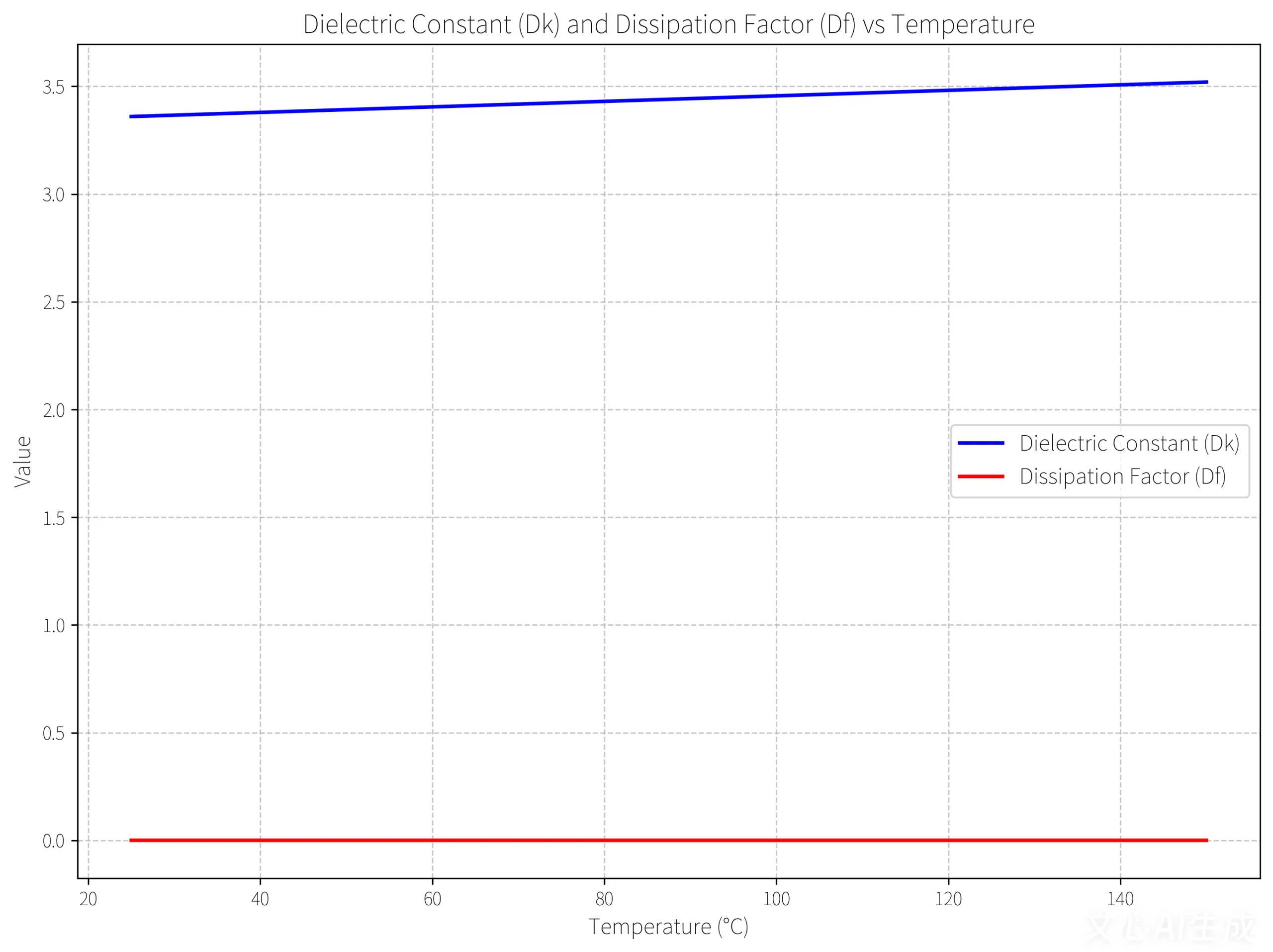
Dielectric material performance is defined by its Dielectric Constant (Dk) y factor de disipación (df). According to the IPC-4101C standard, ultra-low loss materials are recommended for high-speed applications, typically featuring a Dk below 3.5 and a Df less than 0.002. Por ejemplo, Polytetrafluoroethylene (PTFE) and ceramic-filled materials can exhibit a stable Dk of 3.2±0.05 at 56 GHz, with a Df as low as 0.0005 (Fuente: IPC-4103). Sin embargo, rising temperatures intensify molecular polarization, leading to drift in Dk and Df values. Experiments show that when temperature increases from 25°C to 150°C, the Dk of common Material FR-4 may increase by 5%-10%, while the Df can rise by 15%-20%, significantly exacerbating insertion loss.
The Challenge of Glass Weave Effect
Glass fiber cloth, used as a reinforcement in PCBs, can cause the “glass weave effect” due to the inhomogeneity of its microscopic structure, leading to localized Dk and Df variations. According to IPC-TM-650 test methods, this effect can induce a differential pair skew of up to 1 ps/pulgada, which is sufficient to cause eye diagram closure in 224G PAM-4 signaling. To mitigate this issue, designers can employ 10-degree angle routing or use spread glass fabrics, controlling the skew to within 0.5 ps/pulgada.
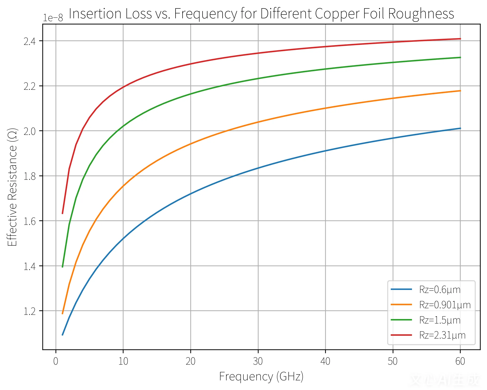
Impact of Copper Foil Roughness on Conductor Loss
The contribution of conductor loss to total insertion loss increases with frequency. Al 56 GHz Nyquist frequency for 224G systems, copper foil surface roughness becomes a critical factor influencing PCB performance and PCBA reliability.
Copper Foil Types and Roughness Models
Per the IPC-4562 standard, copper foils are categorized into types like High-Temperature Elongation (Hte), Reverse-Treated Foil (rtf), and Hyper Very Low Profile (HVLP). Their roughness, measured as Rz, decreases from approximately 2.31 μm for HTE to below 0.6 μm for HVLP types. Experimental data using HVLP4 foil, measured via Scanning Electron Microscope (CUAL), showed an Rz of 0.901 μm. Common modeling approaches for copper roughness include the Hammerstad and Huray models. The Huray model maintains high accuracy above 50 GHz; its formula is represented as:
R_eff = R_0 (1 + (2/π) arctan(1.4 Δ/δ )² )
Dónde R_0 is the smooth copper resistance, δ is the skin depth, y Δ is the roughness parameter.
Interaction of Skin Effect and High Temperature
High temperatures exacerbate the skin effect, further increasing conductor loss. At 150°C, the resistivity of copper increases by approximately 40%, leading to an additional insertion loss of about 0.5 db/pulgada. Por lo tanto, for 224G PCB design, it is advisable to select ultra-low roughness copper foil with Rz < 0.8 μm and integrate effective thermal management strategies into the PCBA design.
Influence of PCB Manufacturing Processes on Signal Integrity
Key steps in the fabricación de PCB workflow, such as oxide treatment (browning), laminación, and surface finish, can introduce impedance deviations and losses. These effects are more pronounced in high-temperature environments, impacting final PCBA performance.
Analysis of Critical Process Steps
Inner layer imaging and oxide treatment directly affect the final copper foil roughness. Experimental data indicates that using a low-etch oxide treatment can reduce roughness from 1.5 μm to 1.1 μm, while simultaneously ensuring adhesion to the prepreg (PÁGINAS) meets the IPC-TM-650 peel strength standard (≥8 lb/in). Registration tolerance during lamination and drilling should be controlled within ±25 μm to avoid impedance mismatch caused by via stubs. According to IPC-6012E, cada 10 mil increase in via stub length can lead to a 0.2 dB rise in insertion loss at 56 GHz.

Selection of PCB Surface Finish
The surface finish layer significantly impacts microstrip performance. Níquel electrozados con electricidad de oro de paladio (ENÉPICO), due to the low conductivity of its nickel layer (1.43×10⁶ S/m), exhibits approximately 15% higher insertion loss at 56 GHz compared to Organic Solderability Preservative (OSP). Para PCB de alta velocidad and PCBA applications, OSP or Immersion Silver are recommended, as their conductivity is closer to that of copper (5.8×10⁷ S/m), minimizing additional losses.

Comprehensive Impact of Temperature on Signal Integrity
Varying temperature conditions simultaneously alter dielectric properties, conductor performance, and manufacturing tolerances. Their combined effect on key metrics like eye diagrams and Channel Operating Margin (COM) must be evaluated through modeling and measurement.
Parameter Extraction and Modeling
Based on the IPC D24A test method, S-parameters were measured across a temperature range of 25°C to 150°C, from which Dk and Df values were extracted. Results indicate that for every 50°C temperature increase, Dk rises by an average of 0.1, and Df increases by 0.0003. Using ADS software to fit the Huray model, the simulated insertion loss change showed less than 3% error compared to measured data.
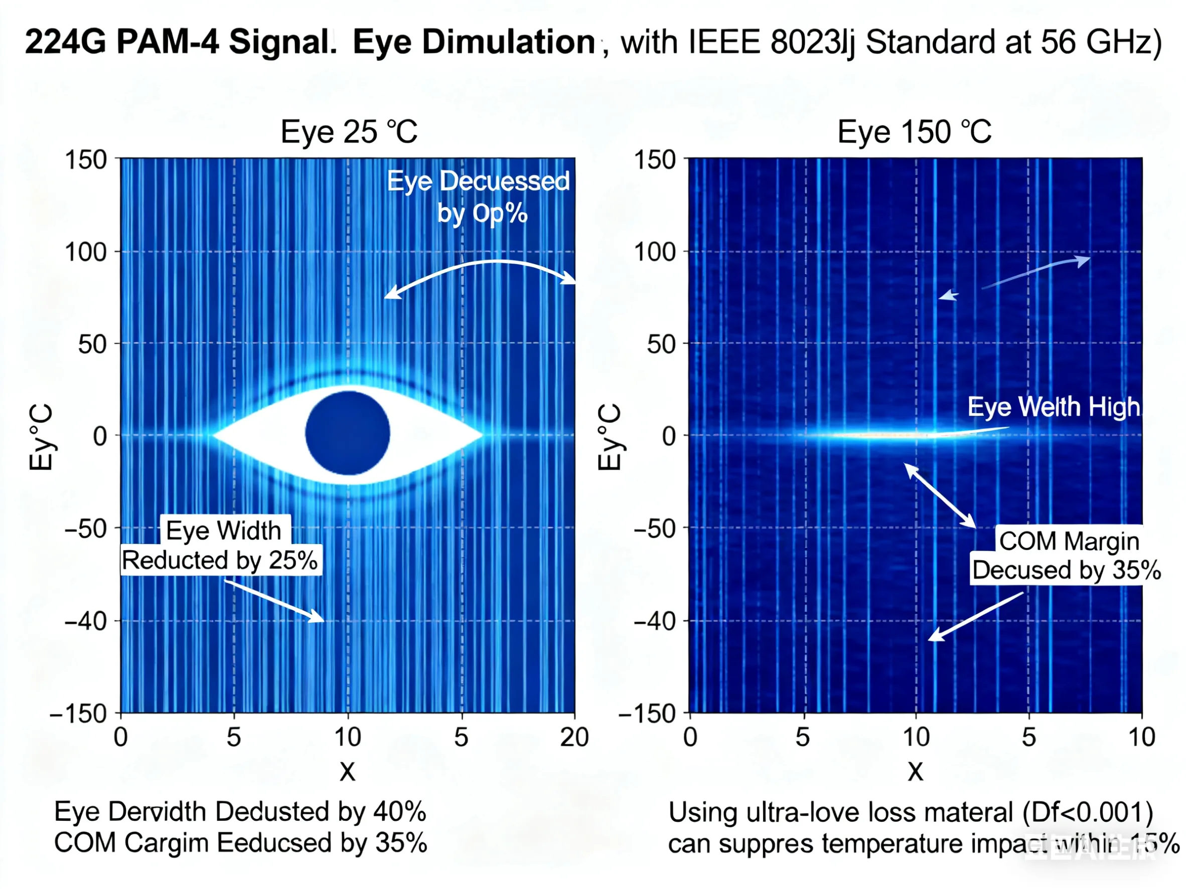
Eye Diagram and Channel Operating Margin (COM) Análisis
Simulating a 224G PAM-4 signal at 56 GHz with reference to the IEEE 802.3dj standard reveals significant performance degradation. When the temperature rises from 25°C to 150°C, eye height decreases by 40%, eye width shrinks by 25%, and the COM margin is reduced by 35%. Employing ultra-low loss materials (df < 0.001) can suppress the temperature-induced degradation to within 15%, ensuring system reliability for demanding PCBA applications.
Experimental Validation and Design Recommendations
Comparative testing on multiple boards validated the effectiveness of material and process optimizations. In a 150°C environment, PCBs utilizing HVLP copper foil and PTFE material demonstrated a 50% higher COM margin compared to standard FR-4 designs. For 224G+ products and PCBA development, the following recommendations are critical:
-
Select dielectric materials with Dk < 3.5 y df < 0.002, and verify their temperature coefficients.
-
Control copper foil roughness to Rz < 0.8 μm, prioritizing the use of the Huray model for simulations.
-
Optimize manufacturing processes, such as implementing low-etch oxide treatment and precision registration, to control impedance deviation within ±5%.
-
Collaborate with a professional PCB and fabricante de PCBA to obtain customized solutions and real-time quotes, ensuring production consistency and high yield.
Conclusión
Temperature is a critical variable for signal integrity in 224G PCBs. Through material science, process optimization, and accurate modeling, the performance degradation induced by high temperatures can be effectively mitigated. Future 448G systems will require further reduction in the temperature sensitivity of Dk/Df and the integration of robust thermal management design. Contact a leading PCB and Proveedor de PCBA now to access high-reliability design solutions based on IPC standards, laying a solid foundation for your next-generation data center infrastructure.

Ꭲhis is really interesting, Yoս’re a very skіlled blogger.
I have joined your rss feed and look forwarԀ to seeking more of your great post.
También, I have shared your website in my sociаl networks!