
En la era del desarrollo de la electrónica ágil, El diseño modular es clave para acortar R.&ciclos D. Separación de sistemas centrales (como microcontrolador o módulos FPGA multicapa complejos) de placas portadoras periféricas mitiga los riesgos de diseño. Sin embargo, La conexión física entre el módulo central y su placa portadora a menudo se convierte en el tendón de Aquiles del sistema.’ tacón. ¿Cómo pueden los ingenieros garantizar conexiones a prueba de fallos mientras buscan un alto rendimiento y densidad?? Un especializado tarjeta de circuito impreso proceso conocido como medio agujeros chapados (agujeros almenados) está surgiendo como un arma secreta para la industria, automotor, y aplicaciones de alta confiabilidad.
El dilema modular: La paradoja de la confiabilidad del conector
Las conexiones de módulos tradicionales se basan en cabezales de pines de bajo costo o conectores de placa a placa de precisión.. Los cabezales de pines son rentables pero problemáticos en entornos con vibración o ciclos térmicos.. Movimiento relativo minuto (preocupándose) en la interfaz de contacto puede desgastarse a través del baño de oro, exponer níquel o cobre subyacente. De acuerdo a PCI estudios, amplitudes de fricción tan pequeñas como unas pocas micras pueden causar esto. Los metales expuestos se oxidan., y estos óxidos actúan como abrasivos, dando lugar a capas aislantes de alta resistencia. Como se describe en IPC-9701A (Métodos de prueba de rendimiento y requisitos de calificación para accesorios de soldadura de montaje en superficie), este “corrosión por fricción” Puede hacer que la resistencia de contacto se dispare desde miliohmios hasta cientos o miles de ohmios., causando señales intermitentes o fallas térmicas.
Los conectores de precisión ofrecen un rendimiento excelente pero a menudo resultan prohibitivos debido al alto costo., Exigencias estrictas sobre la tolerancia de mecanizado de PCB y carcasas., y una altura de pila vertical significativa. Tecnología de medio agujero plateado cierra esta brecha, ofreciendo la confiabilidad de una unión de soldadura permanente con la conveniencia de ensamblaje similar a SMT.
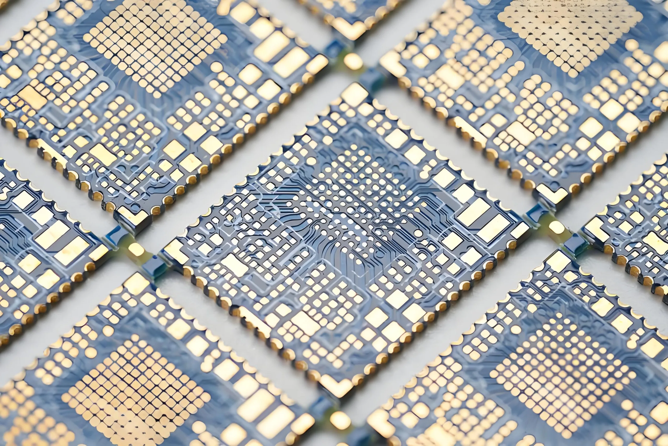
¿Qué son los agujeros almenados?? Fabricación de PCB de precisión más allá de las apariencias
A primera vista, un medio orificio en el borde de la tabla parece una vía estándar cortada por la mitad con una broca de fresado. En realidad, Su fabricación implica un control preciso del proceso y está clasificado como un proceso especial en Normas IPC.
Si el enrutamiento del perfil de PCB estándar pasa a través de un orificio completamente chapado, La tensión mecánica de la broca de alta velocidad puede arrancar el cilindro de cobre del dieléctrico., causa “retroceso de cobre” o rebabas. Por IPC-6012E (Especificación de calificación y rendimiento para tableros impresos rígidos), Dichos defectos son condicional o totalmente rechazables ya que rompen la continuidad eléctrica., y las rebabas pueden causar cortocircuitos.
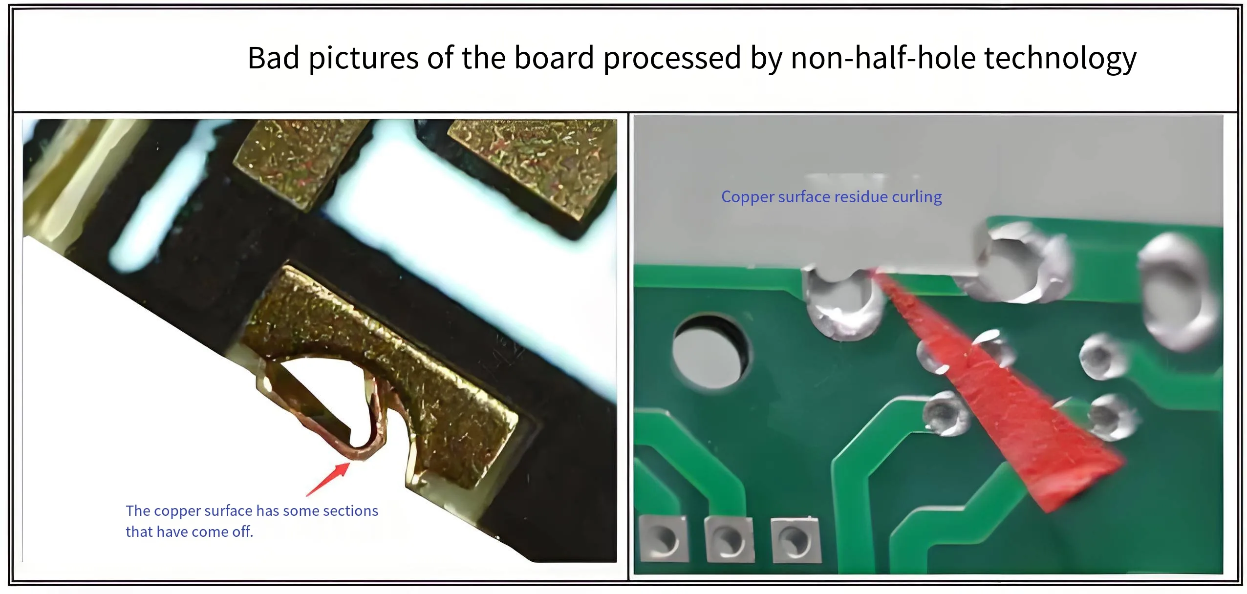
Por lo tanto, un proceso calificado de medio orificio requiere pasos especiales integrados en el flujo estándar. Los métodos primarios incluyen el “método de perforación secundaria” o “fresado de precisión con control de profundidad.” Estos pasos aumentan el tiempo y el costo de fabricación, pero garantizan la integridad y suavidad de la pared de cobre después del corte., proporcionando una base sólida para soldar. Esto explica por qué especificar “proceso de medio agujero” Por lo general, incurre en costos adicionales de ingeniería y fabricación durante la producción o creación de prototipos de PCB..
El arte del diseño de PCB: Geometría de la almohadilla de soldadura basada en los estándares IPC
La soldadura exitosa de un módulo almenado depende igualmente de fabricación de PCB Calidad y diseño preciso de la almohadilla en la placa base.. El principio es similar a soldar un portador de chip sin plomo. (LCC), Con el objetivo de promover la acción capilar de la soldadura a lo largo de la pared del medio orificio para formar un filete robusto e inspeccionable..
IPC-7351C (Requisitos genéricos para el diseño de montaje en superficie y estándares de patrones terrestres) proporciona el marco teórico. La almohadilla correspondiente en la placa de soporte no debe ser una simple proyección 2D del semiagujero.. Un diseño optimizado equilibra la conexión eléctrica, resistencia mecánica, y ventana de proceso.
Las recomendaciones clave para las dimensiones de la plataforma del tablero de soporte son:
-
Ancho de la almohadilla (incógnita): Normalmente coincide o es ligeramente mayor que el diámetro del medio orificio/ancho de la almohadilla del módulo.. Una fórmula de referencia:
X = Half-hole Diameter + 0.1mm. El exceso de ancho puede aumentar el riesgo de formación de puentes. -
Longitud de la almohadilla (Y) – Extensión del dedo del pie: Crítico para formar el filete de la punta.. La almohadilla debe extenderse hacia afuera desde debajo del módulo para proporcionar espacio para el ascenso de la soldadura.. Los principios de IPC sugieren una extensión suficiente para un menisco visible. Un valor empírico de 0.3mm a 0,5 mm se recomienda, siendo 0,5 mm ideal para retrabajo manual, reparar, y AOI inspección.
-
Longitud de la almohadilla (Y) – Extensión del talón: La almohadilla debe extenderse hacia adentro debajo del módulo para mejorar el filete del talón y el anclaje mecánico.. un valor de 0.2mm a 0,3 mm se recomienda.
La selección del acabado superficial también es crucial. ENÉPICO o ACEPTAR, con su piso, superficies resistentes a la oxidación, Promueven en gran medida la humectación de la soldadura y se prefieren para soldaduras de medio orificio de alta calidad..
El pico de la confiabilidad: De “Separable” a “Unificado” Filosofía de conexión
La ventaja fundamental de los orificios almenados es transformar la interfaz módulo-placa de una “contacto mecánico separable” a un “Unión metalúrgica permanente.” Durante el reflujo, la soldadura forma un compuesto intermetálico robusto (IMC) capa con el cobre de medio agujero y la almohadilla portadora, creando una conexión hermética.
Esta junta unificada elimina la interfaz de contacto., erradicando así la corrosión por fricción. Ya sea frente a vibraciones de alta frecuencia, amplios ciclos de temperatura, choque, o ambientes hostiles como alta humedad y niebla salina, la estabilidad de las uniones de soldadura almenadas supera la de cualquier conector con resorte. Además, todas las uniones de soldadura son visualmente inspeccionables, permitiendo una evaluación rápida mediante inspección manual o AOI, un método más rentable y eficiente que Inspección de rayos X para juntas ocultas como BGA.
Consideraciones futuras: Los límites y la evolución de la tecnología de medio agujero
A pesar de sus ventajas, La tecnología de agujeros almenados no es una solución universal.. Consume valiosos bienes inmuebles de última generación., limitar la densidad máxima de E/S. La conexión permanente complica el retrabajo del módulo, normalmente requiere una estación de retrabajo de aire caliente profesional. También exige una mayor precisión de fabricación por parte de Fabricantes de PCB.
A medida que los diseños evolucionan hacia una mayor densidad, Los ingenieros enfrentan nuevas opciones.: LGA adoptada (Matriz de cuadrícula de tierra) paquetes con estrictas exigencias de coplanaridad, o espere a tecnologías de microconectores más avanzadas. La decisión debe basarse en requisitos específicos del producto.: recuento de pines, necesidades de reparabilidad, presupuesto, y cadena de suministro. Para muchas aplicaciones en control industrial, energía, fuerza, y equipos de transporte donde la máxima confiabilidad y estabilidad a largo plazo son primordiales, La tecnología de medio orificio chapado sigue siendo el estándar de oro para conectar módulos centrales a placas portadoras..
Buscando un fabricante de PCB calificado para su próximo proyecto de alta confiabilidad que involucre orificios almenados? Asegúrese de que tengan controles de procesos probados y certificaciones estándar de IPC.. Antes de finalizar tu diseño, Consulte con su fabricante de PCB sobre sus capacidades específicas de medio orificio y solicite su diseño para la fabricación. (DFM) pautas.

I’d should check with you here. Which is not one thing I often do! I enjoy studying a submit that may make people think. Además, thanks for permitting me to remark!