
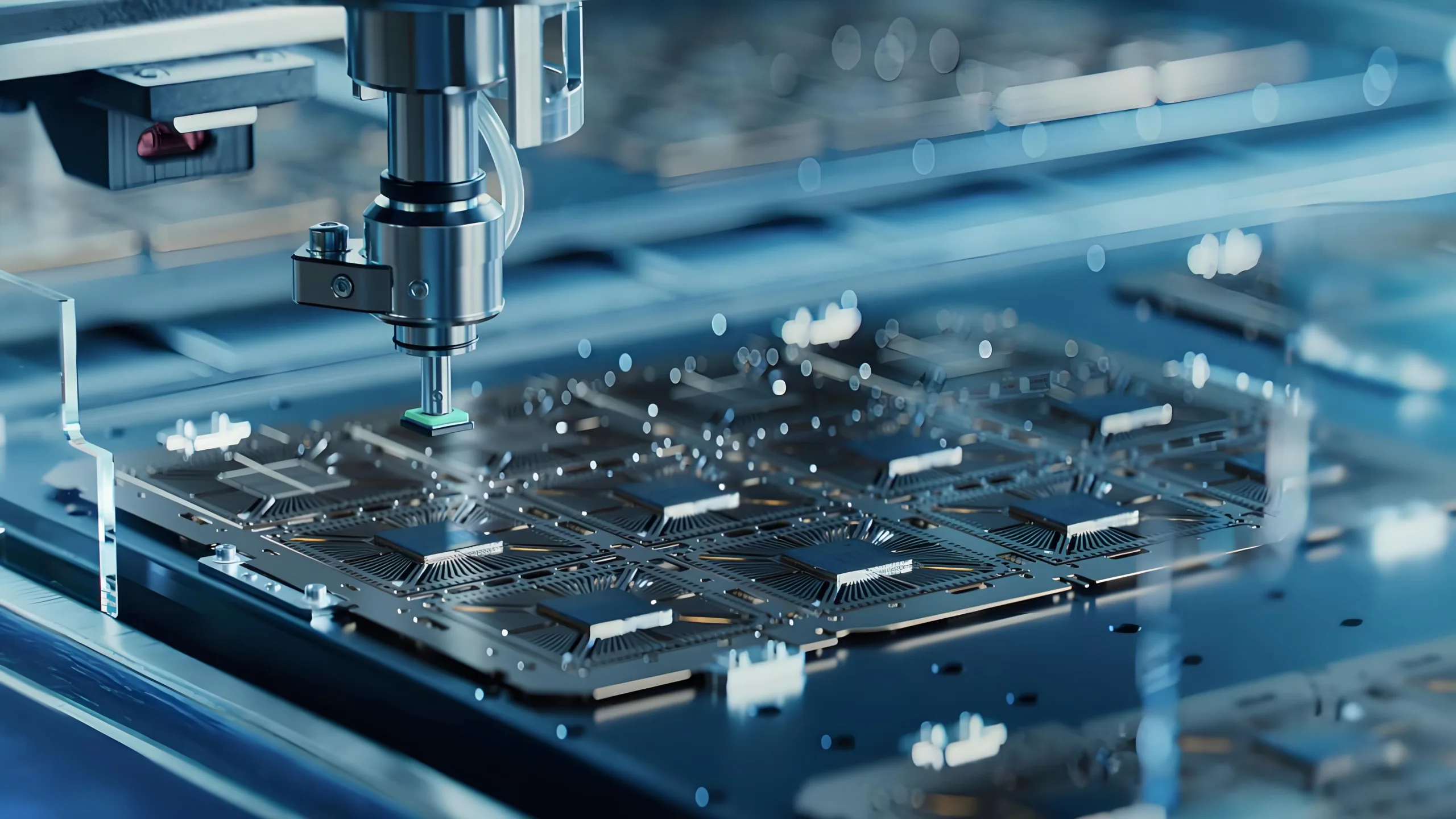
Los chips de semiconductores sirven como el “sesos” de la era digital, mientras que el empaque de chips actúa como su protección “armadura” y “Red neuronal.” Más allá de la muerte de silicio frágil de blindaje, Permite una gestión térmica crítica, conectividad eléctrica, y transmisión de señal. Desde paquetes voluminosos de agujeros hasta soluciones de nivel de oblea ultra delgada, La evolución del empaque ha impulsado la miniaturización electrónica y la mejora del rendimiento: una saga tecnológica monumental.
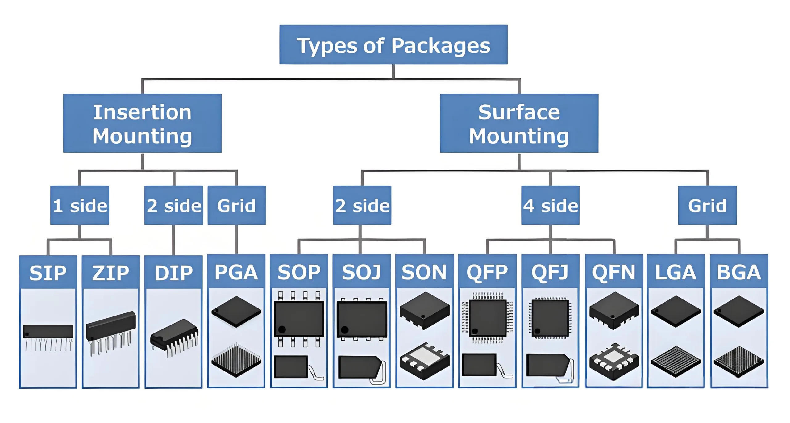
Clasificación de tecnologías de embalaje
Por método de montaje
-
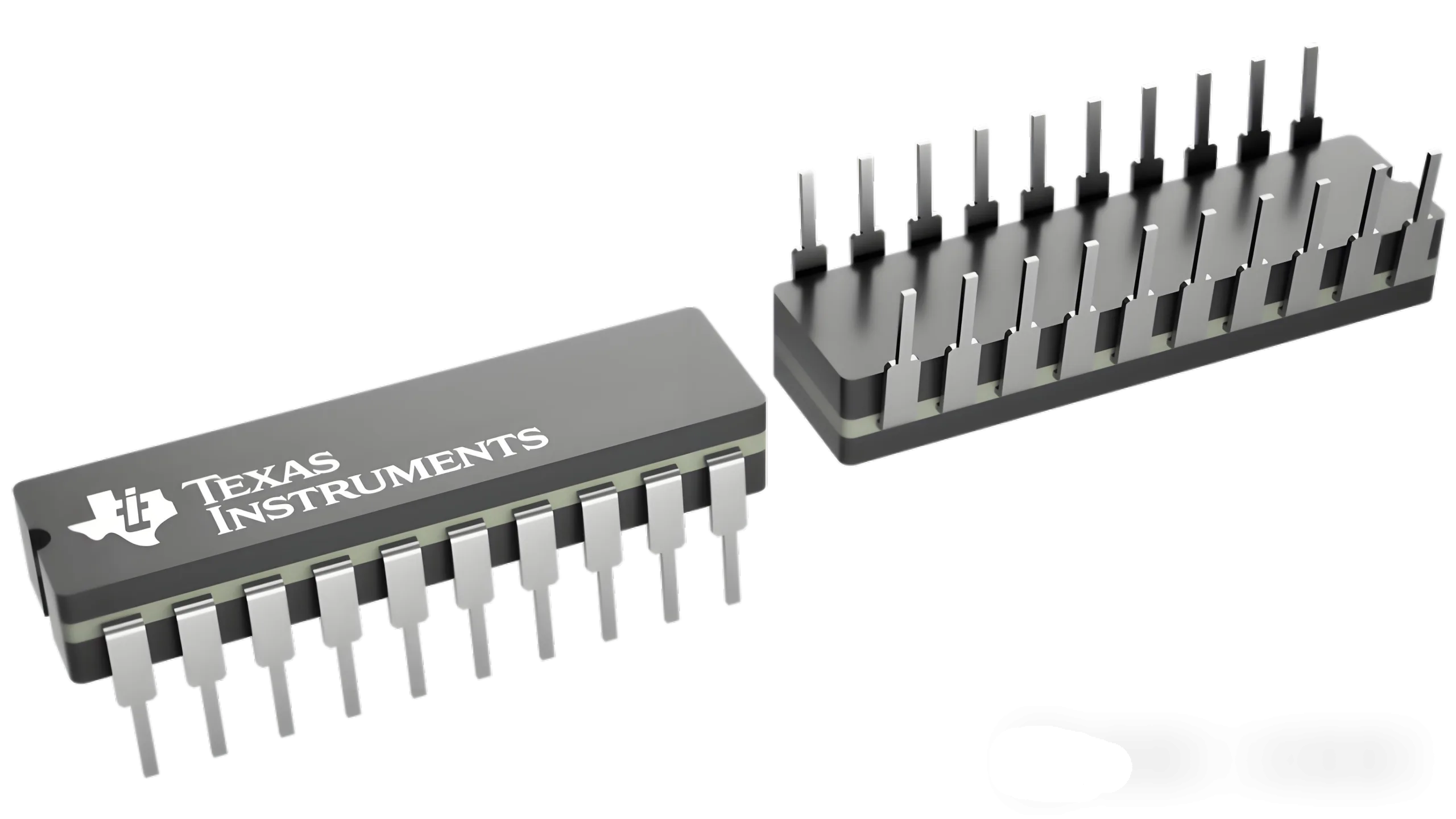
Envasado de agujeros (Tht):
Pines insertados en tarjeta de circuito impreso a través de los agujeros para soldar. Representa la tecnología de generación temprana. -
Tecnología de montaje en superficie (SMT):
Componentes soldados directamente en almohadillas para PCB. Habilita una mayor densidad y ensamblaje automatizado.
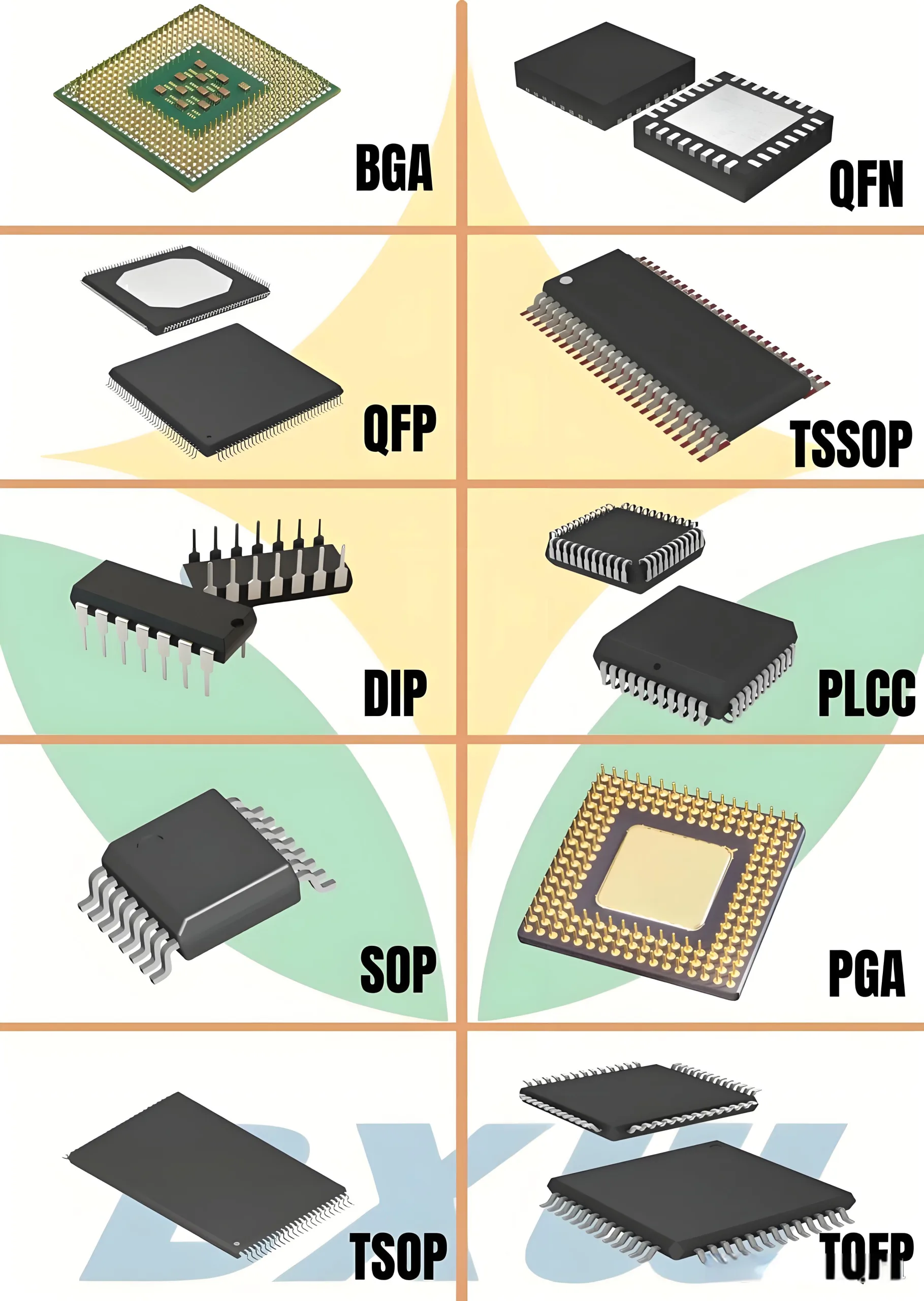
Por configuración de pin (Progresión de densidad)
Single-Row → Dual-fila → Quad-lado → Array de área
La era del agujero
Hacer/a: Fundamentos de componentes discretos
-
Diodo do-41: Ø2.7 mm × 5.2 mm
-
Transistor de 220: Maneja la disipación de potencia ≤50W
-
Resistencia térmica: R<sub>y</sub> = (t<sub>j</sub> – t<sub>a</sub>)/PAG
Dónde R<sub>y</sub> = Resistencia térmica de unión a ambiente
Dar una paliza a: Innovaciones individuales en línea
-
SORBO: 3-16 patas, rentable para resistencias/diodos de baja potencia
-
CREMALLERA: 40% Densidad de pasador más alta que SIP a través de la disposición del pasador de zigzag
-
Aplicaciones: Módulos de memoria tempranos, reguladores de voltaje
ADEREZO: La revolución de IC
-
Pitch: 2.54milímetros (0.1″) estándar
-
1980s cuota de mercado: >70% de embalaje IC
-
Rendimiento térmico:
Salsa de cerámica: 20-30 W/m · k conductividad
Salsa de plástico: 0.2-0.3 W/m·K
PGA: Pionero informático de alto rendimiento
-
Densidad: 3× más alto que la inmersión
-
Aplicaciones: Intel 80386/80486 CPU
-
Fuerza de inserción: 30-100 Newtons
La revolución SMT
Sod: Miniaturización de componentes discretos
-
Sod-323: 1.7mm × 1.25 mm
-
SOT-23 Resistencia térmica: ~ 250 ° C/W
-
Perfil de reflujo: Temperatura máxima 235-245 ° C
Proporciona el ala de la gaviota: Familia SOP
-
Evolución de Pin Pitch:
1.27milímetros (COMPENSACIÓN) → 0.8 mm (SSOP) → 0.65 mm (Tssop) -
Paquetes derivados:
SOP → SSOP → TSOP → TSSOP → VSSOP -
Mejora térmica: HSSOP reduce la resistencia térmica por 40%
Configuración de J-LEAD: Observación
-
Resistencia mecánica: 30% mayor resistencia al estrés
-
Limitación eléctrica: 0.8-1.2NH inductancia parásita
Avance sin plomo: Hijo/DFN
-
Eficiencia del espacio: >50% Mejora sobre SOP
-
Rendimiento térmico: 15° C/W con almohadillas térmicas
-
Límite de miniaturización:
X2son: 0.6mm × 0.6 mm × 0.32 mm
Física detrás de la miniaturización
Tres desafíos básicos gobiernan la escala de paquetes:
-
Gestión Térmica:
Q = haΔt
Tamaño reducido (↓ A) exige un mayor coeficiente de convección (↑ H) -
Control del estrés térmico:
S = EPTT
Donde cte (a) El desajuste induce el estrés -
Integridad de señal:
Inductancia de plomo *l ≈ 2l(LN(2L/D)-1) Nueva Hampshire*
La miniaturización reduce la inductancia por 30%
Siguiente frontera: Embalaje avanzado
Como x2son alcanza escamas de 0.6 mm, La innovación cambia a:
-
3D Embalaje: Integración vertical habilitada para TSV
-
Integración heterogénea: Ensamblaje de diedes múltiples
-
Fotónica: Codsign de Silicon Photonics
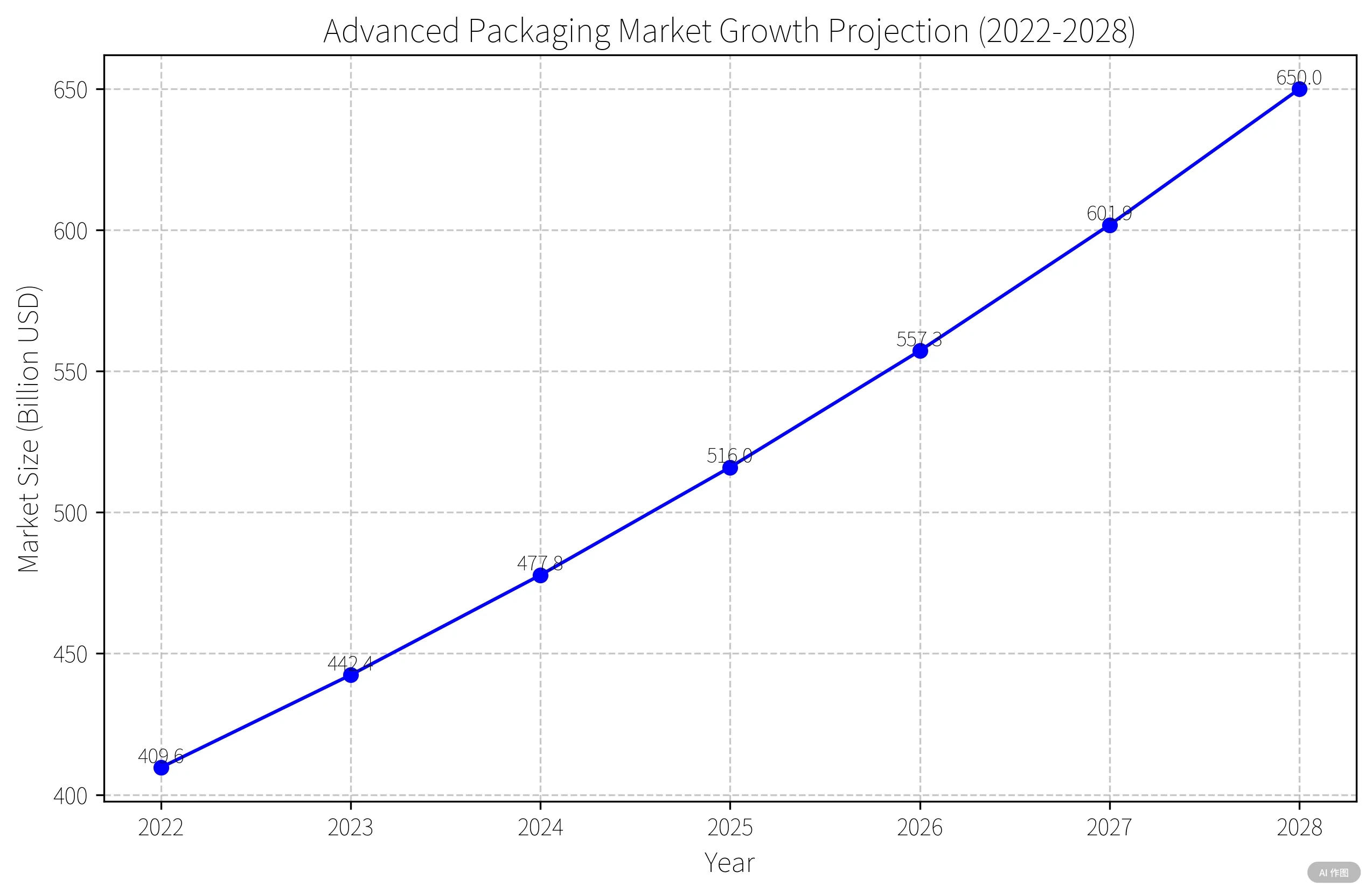
Pronóstico del mercado (Yole DevelovelPement):
8% CAGR a través de 2028 → mercado de $ 65B
El embalaje ahora define críticamente el rendimiento del sistema: mucho más allá de la mera protección.
Conclusión
Desde el tono de 2.54 mm de DIP hasta la huella de 0.6 mm de X2son, Los avances de empaque redefinen continuamente la electrónica. Cada teléfono inteligente delgado y dispositivo 5G depende de estas innovaciones invisibles. Con IA y computación cuántica emergente, El embalaje de chips seguirá empujando los límites a nanoescala.
*Siguiente en serie:
Tecnologías BGA/CSP/WLCSP
3D Embalaje & Interconexiones de TSV
Ciencia de materiales de embalaje avanzado
Manténganse al tanto!*
