
La batalla de vida o muerte en microelectrónica: Reacción en cadena inducida por la brecha de máscara de soldadura
Con 0201 componentes y bgas de tono de 0.3 mm que se convierten en la corriente principal, tarjeta de circuito impreso tarifas de omisión de soldadura han surgido 37% (PCI 2023 datos). De acuerdo con un estudio de una década por UGPCB: 60% de defectos SMT se originan en la falla de transferencia de pasta, dónde brechas de impresión de micro almohadillas actuar como los pasados por alto “asesino invisible”.
Lecciones escritas en sangre: La micrografía revela puntos de dolor de la industria
-
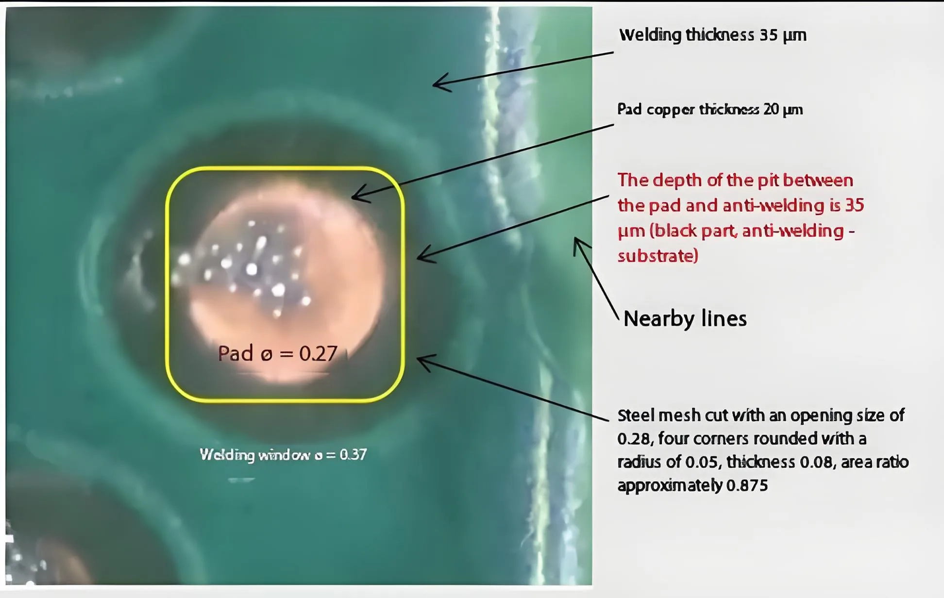
Máscara de soldadura a la altura de la almohadilla de cobre: 35μm
-
Aperture de plantilla que cubre el área de sustrato: 42%
-
Área de contacto de pasta de soldadura efectiva: <58%
Física detrás del fracaso: Lo matemático “Triángulo de la muerte” de transferencia de pasta
Fórmula fatal: El colapso de la teoría de la relación de área IPC-7525
Relación de área = (L × W) / [2H(L+W)]
La teoría tradicional falla cuando el diámetro de la almohadilla ≤0.3 mm! Los datos empíricos de los principales fabricantes revelan:
| Diámetro de la almohadilla (milímetros) | Relación teórica | Tasa de transferencia real |
|---|---|---|
| 0.40 | 0.68 | 92% |
| 0.31 | 0.61 | 85% |
| 0.27 | 0.55 | 63% |
Dinámica de fluidos expuesto: Por qué la pasta de soldadura “Rechazado” Almohadilla
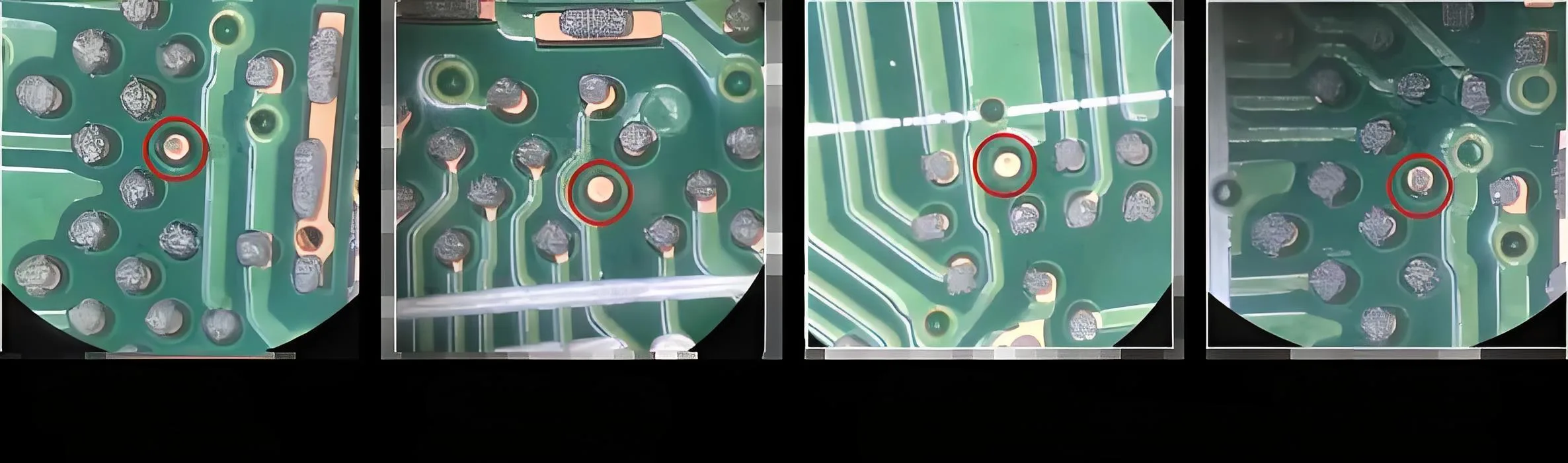
Cifra 2: Simulación de tensión fluida durante la liberación de plantilla
Alternativo: Análisis de tensión de la pared de la plantilla de pasta de soldadura – Simulación de defectos de impresión PCBA – Soluciones SMT
Hallazgos críticos:
-
Los huecos de máscara de soldadura crean efecto de cojín de aire, Reducir el área de contacto por 41%
-
El salto de soldadura ocurre cuando la cohesión de pasta > adhesión
Soluciones de grado industrial: Tres pilares para eliminar la soldadura omitiendo
Revolución del diseño de la almohadilla: Principio de expansión del cobre
-
Diámetro aislado de la almohadilla: 0.27mm → 0.31 mm
-
Cobertura de brecha reducida a 12%
-
La tasa de transferencia aumentada a 89% (datos empíricos)
Máscara de soldadura “Adelgazante” Iniciativa: El estándar de oro de 25 μm
Cifra 3: Comparación de impresión con diferentes espesores de máscara de soldadura
Alternativo: Comparación de espesor de máscara de soldadura de PCB – Mejora del rendimiento de SMT – Guía de proveedores de PCBA
Fórmula de grosor: H = (RZ + d) × K
(δ = Tamaño de partícula de pasta, Tipo 4: 25μm; K = factor de seguridad 1.2)
Validación de la industria: El fabricante de PCB móvil redujo el grosor de 35 μm a 22 μm → 82% Reducción en el salto de soldadura de QFN
Plantillas de ph: La mejor solución de nano-conformidad
 Innovación:
-
Diseño de apertura escalonada: Ángulo de pared de 7 ° a 15 °
-
Níquel electroformado: 3x aumento de dureza
-
Ángulo de asistencia de demoldización: 40% fricción de pared reducida
Líderes de la industria’ Libro de jugadas: IDH + Norma de oro NSMD
Estrategia de precisión de la industria móvil
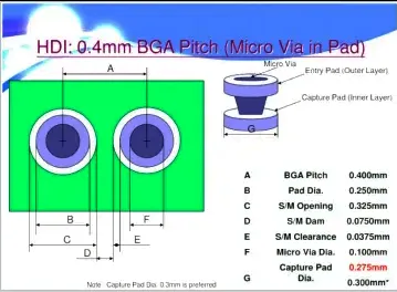
Caso: 0.4MM Pitch BGA Process Blueprint
1. Reemplace la impresión de leyenda → diseño de cobre desnudo
2. Implementar IDH Microvias
3. Grosor de la máscara de soldadura: 18± 3 μm (Clase IPC-6012 3 obediente)
Motor de conversión: Su plan de acción de actualización de fábrica
Lista de verificación de ejecución inmediata:
-
Auditar todas las almohadillas aisladas: Rediseño si diámetro <0.3milímetros
-
Demanda de los informes de grosor de máscara de soldadura de Proveedores de PCB (Métrica clave: ≤25 μm)
-
Adquirir plantillas de pH con urgencia: 55% ganancia de eficiencia de apertura en áreas de lanzamiento fino
