Diseño de PCB, Fabricación de PCB, tarjeta de circuito impreso, PEVD, y selección de componentes con un servicio único

Descargar | Acerca de | Contacto | Mapa del sitio

Diseño de PCBA HDI de interconexión arbitraria - UGPCB

Diseño de PCB HDI/

Diseño de PCBA HDI de interconexión arbitraria

Nombre: Diseño de PCBA HDI de interconexión arbitraria

Lámina: TG170 /TG180, F4BM, FR4, FR1-4, etc..

Capas diseñables: 1-32 capas

Ancho de línea mínimo y espacio entre líneas: 3mil

Apertura mínima del láser: 4mil

Apertura mecánica mínima: 8mil

Espesor de la lámina de cobre: 18-175centímetro (estándar: 18cm35cm70cm)

Fuerza de pelado: 1.25N/mm

Diámetro mínimo del agujero de perforación: un solo lado: 0.9mm/35mil

Diámetro mínimo del agujero: 0.25mm/10mil

Tolerancia de apertura: ≤φ0,8 mm ±0,05 mm

Tolerancia del agujero: ±0,05 mm

Hole wall copper thickness: double-sided/multi-layer: ≥2um/0.8mil

Hole resistance: double-sided/multi-layer: ≤300цΩ

Ancho mínimo de línea: 0.127mm/5mil

Minimum pitch: 0.127mm/5mil

Screen printing color: negro, blanco, rojo, verde, etc..

Tratamiento superficial: lead/lead-free tin spray, ACEPTAR, silver, OSP

Servicio: Provide OEM service

Certificate: ISO9001.ROSH.UL

  • Detalles del producto

Any Layer HDI PCB: The Most Complex Design Structure

Descripción general

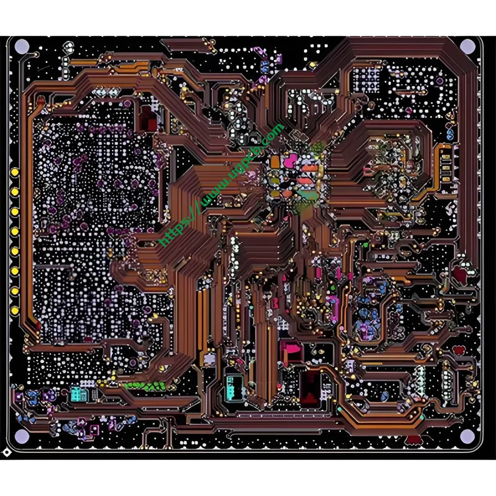
Any Layer HDI PCB is the most complex HDI PCB design structure, offering unparalleled connectivity and performance.

High-Density Interconnect Layers

All Layers as HDI

In this structure, all layers are high-density interconnect layers, allowing for free interconnection of conductors on any layer of the PCB.

Copper-Filled Stacked Microvia Structure

The copper-filled stacked microvia structure facilitates this interconnectivity, providing a reliable and efficient means of connecting various layers.

Aplicaciones

Highly Complex Devices

This structure is ideal for highly complex, high pin-count devices such as CPU and GPU chips used in handheld and mobile devices.

Excellent Electrical Characteristics

The design yields excellent electrical characteristics, haciéndolo adecuado para aplicaciones de alto rendimiento.

Beneficios

Reliable Interconnect Solution

The Any Layer HDI PCB structure provides a reliable interconnect solution for complex devices, ensuring stable and efficient performance.

UGPCB Advantage

This structure, featuring UGPCB technology, represents a significant advancement in PCB design and manufacturing.

Anterior:

Próximo:

Deja una respuesta

Dejar un mensaje