
Descripción general del producto: What is an HDI IC Substrate Board?
An HDI IC Substrate Board is a critical, high-end placa de circuito impreso engineered specifically for semiconductor package interconnection. It acts as the essential interface, providing electrical connectivity, distribución de energía, and mechanical support between a finely-pitched silicon die and a standard motherboard tarjeta de circuito impreso. UGPCB delivers high-reliability, advanced HDI IC Substrate manufacturing, meeting the stringent demands of applications from consumer electronics to high-performance computing.
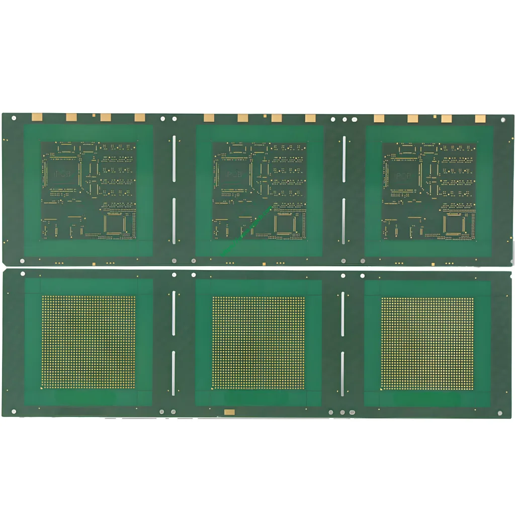
This board, built with SI10U material in a 6-capa (2+2+2) construction and a slim profile of 0.6milímetros, exemplifies state-of-the-art IDH tecnología. With a 35x35mm unit size, it features a 0.1mm minimum laser via diameter, 30μm minimum trace width / 70μm minimum spacing, y ENÉPICO (Níquel electrozados con electricidad de oro de paladio) acabado superficial, making it an ideal solution for packaging high-speed, de alta frecuencia, and highly integrated chips.
In-Depth Analysis: Diseño, Función, and Applications
Core Definition & Principio de trabajo
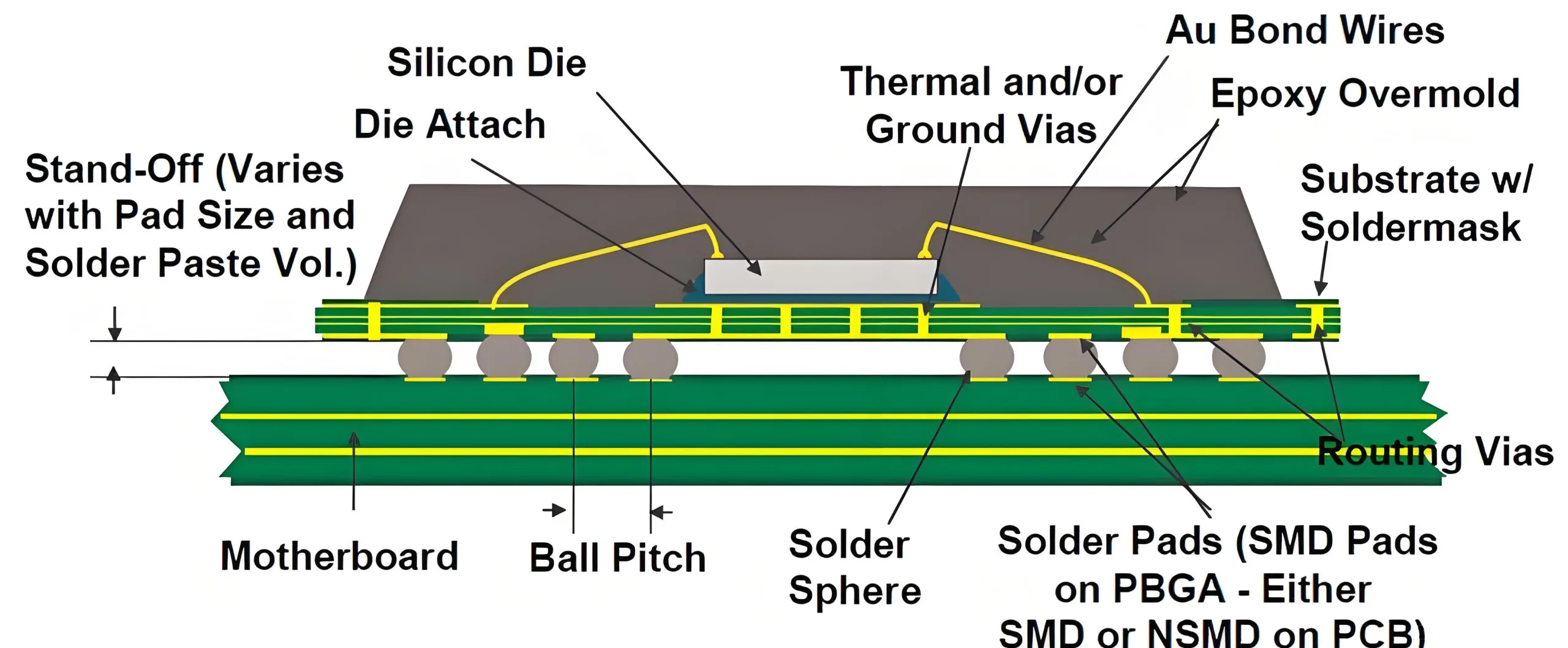
The HDI IC Substrate is designed to “fan-out” the dense array of micro-bumps from a semiconductor die, redistributing the connections to a larger pitch compatible with standard ensamblaje de PCB processes like BGA (Matriz de rejilla de bolas) montaje.
The working principle follows this chain: Die → Microbumps → HDI IC Substrate (for signal redistribution & interconexión) → Solder Balls (BGA/CSP) → Mainboard PCB. It is pivotal for signal integrity, power delivery, y gestión térmica.
Key Design Considerations
-
Stack-up & Control de impedancia: The 6-layer (2+2+2) build-up is a classic design for high routing density. Precise impedance calculation (typically 50Ω single-ended or 100Ω differential) is crucial for signal integrity.
-
Micro-via Reliability: 0.1milímetros (100μm) laser-drilled micro-vias are key for interconnect density. Via shape, recubrimiento de cobre, and fill process must be optimized for thermal cycle reliability.
-
Fine-Line Fabrication: 30μm trace width and 70μm spacing are core metrics of process capability, directly impacting I/O density and electrical performance.
-
Thermal & Mechanical Management: The selection of SI10U material considers its Coefficient of Thermal Expansion (CTE) matching with silicon to minimize thermal stress and enhance product longevity.
Primary Materials & Características de rendimiento
-
Material central: SI10U. A high-performance laminate offering low dielectric constant (Dk), low dissipation factor (df), high glass transition temperature (tg), and excellent dimensional stability, ideal for high-speed, high-frequency applications.
-
Máscara de soldadura: PSR-4000 AUS308. A high-resolution, high-reliability Liquid Photoimageable Solder Mask (LPSM) that provides precise coverage, excellent insulation, and chemical resistance.
-
Acabado superficial: ENÉPICO. This finish deposits sequential layers of Nickel, Palladium, and Gold. Nickel acts as a diffusion barrier, Palladium prevents nickel corrosion, and the thin gold layer offers superior solderability and wire-bonding capability, perfect for fine-pitch pads.
-
Performance Summary: Densidad alta, alta velocidad, alta confiabilidad, Excelente gestión térmica, and superior signal integrity.
Clasificación & Escenarios de aplicación
HDI IC Substrates are categorized by technology and application:
-
Por tecnología: With core (p.ej., this 6L build-up) or coreless types.
-
Por aplicación:
-
Advanced Processors: UPC, GPU, AI accelerator chips requiring maximum routing density and signal speed.
-
Mobile & RF: Smartphone Application Processors (AP) y módulos de RF, where miniaturization and thin profiles (0.6milímetros) are critical.
-
Memoria: Interface substrates for High Bandwidth Memory (Hbm).
-
Networking & Automotor: High-speed switch chips and ADAS domain controllers.
-
UGPCB’s Manufacturing Process & Seguro de calidad
UGPCB’s production integrates leading-edge processes compliant with IPC standards:
-
Perforación láser: UV laser systems create precise 0.1mm micro-vias.
-
Enchapado & Via Fill: Advanced pulse plating ensures complete via filling for reliable interconnects.
-
Advanced Imaging: High-end exposure systems and high-resolution dry film achieve 30/70μm line definition.
-
Laminación: Precise alignment and pressing of multiple core layers and prepreg (PÁGINAS).
-
Acabado de superficies: Application of the ENÉPICO coating for optimal solderability.
-
Prueba integral: Utilizes AOI (Inspección óptica automatizada), Prueba de sonda voladora, and impedance testing to guarantee compliance.
Nuestro one-stop tarjeta de circuito impreso servicio capability extends from sustrato CI fabricación to subsequent Ensamblaje SMT y pruebas, offering a complete packaging solution.
Why Choose UGPCB for Your HDI IC Substrate?
-
Advanced Process Capability: Proven expertise in 30/70μm trace/space y 0.1mm micro-via tecnología.
-
Materials Expertise: In-depth knowledge of advanced materials like SI10U to recommend optimal solutions.
-
Uncompromising Quality: Stringent, automotive-grade quality control throughout the entire process.
-
One-Stop Solution: We are more than a PCB fabricator; we are your PCBA partner, offering design support, fabricación, y montaje.
-
Expert Support: Dedicated engineering team provides DFM (Diseño para la fabricación) analysis and technical consultation.
Obtenga su solución personalizada ahora
Whether you are developing the next HPC platform, 5G Infraestructura, o ADAS system, UGPCB’s professional HDI IC Substrate manufacturing y Servicios de montaje de PCBA are your foundation for success.
Contact us today for a free technical consultation and quote! Let our experts help you enhance product performance through optimized IC substrate design and reliable fabricación de PCB procesos.


