
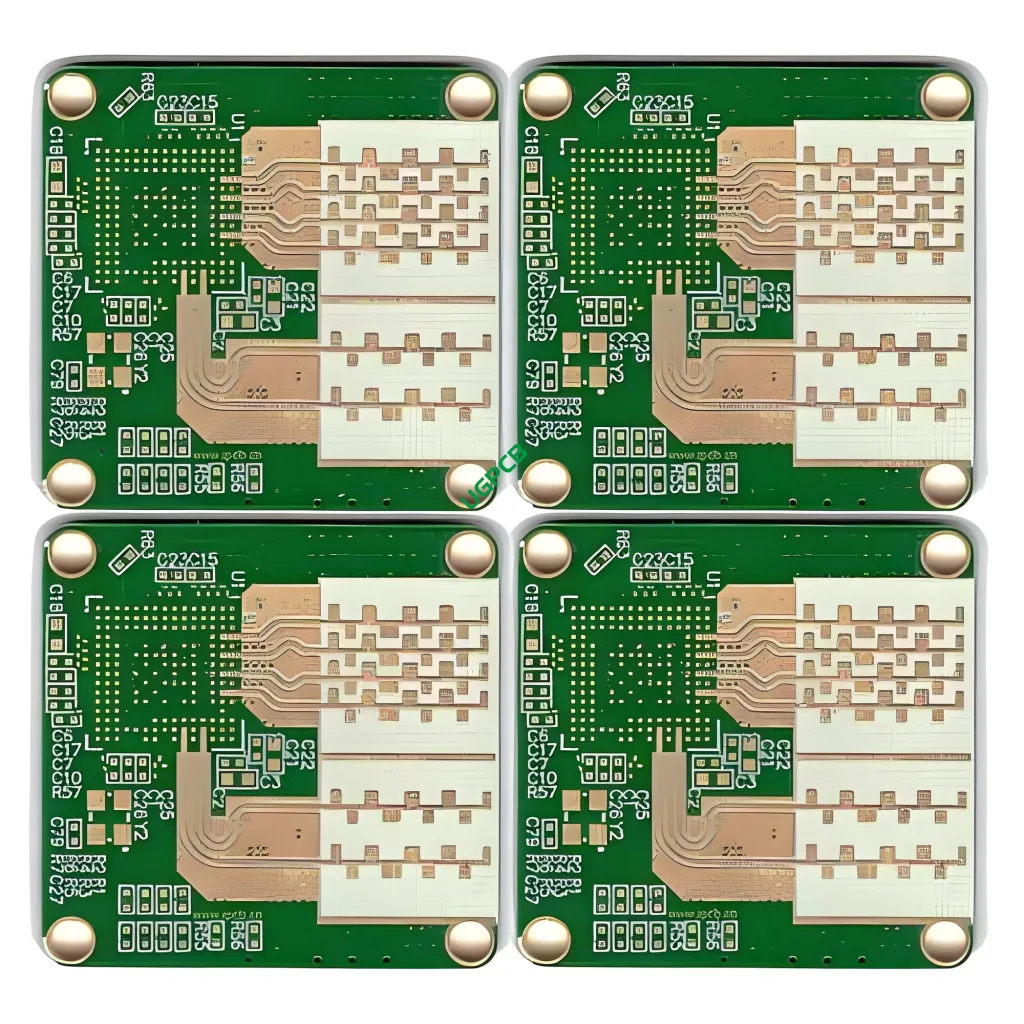
Descripción general de PCB de alta frecuencia
A PCB de alta frecuencia is a specialized type of circuit board designed to operate at high frequencies, típicamente en el rango de gigahertz (GHz). Estos PCB son esenciales para aplicaciones que requieren una transmisión de señal precisa y una pérdida de señal mínima. Se utilizan ampliamente en industrias como las telecomunicaciones, sistemas de radar, y comunicaciones satelitales. El estándar de calidad para PCB de alta frecuencia es IPC 6012 Clase 2, Garantizar una alta fiabilidad y rendimiento.
Definición y especificaciones clave
Una PCB de alta frecuencia se define por su capacidad para manejar señales a frecuencias muy altas mientras mantiene la integridad de la señal. La constante dieléctrica (dk) de estos PCB varían desde 2.0 a 1.6, que es crucial para controlar la velocidad de la señal y la impedancia. El número de capas puede variar de 1 a 36, proporcionar flexibilidad para diferentes requisitos de diseño. El grosor de la PCB varía de 0.254 mm a 12 mm, y el grosor de cobre puede ser de 0.5 oz o 1 oz. Las tecnologías de superficie incluyen plata, Oro, y OSP, Cada uno ofrece diferentes beneficios en términos de soldadura y resistencia a la corrosión. Los procesos especiales como materiales mixtos y surcos escalonados mejoran aún más el rendimiento de los PCB de alta frecuencia.
Consideraciones de diseño
Al diseñar una PCB de alta frecuencia, Se deben considerar varios factores:
- Constante dieléctrica (dk): El valor dk entre 2.0 y 1.6 es crítico para mantener la integridad de la señal a altas frecuencias.
- Número de capas: La amplia gama de opciones de capa (1 a 36) Permite la personalización basada en necesidades de aplicación específicas.
- Espesor: El rango de grosor de 0.254 mm a 12 mm proporciona flexibilidad en el diseño, atender a diferentes requisitos espaciales y funcionales.
- Espesor de cobre: La elección entre el cobre base de 0.5 oz y 1 oz afecta la capacidad de transporte de corriente y la integridad de la señal.
- Tecnología superficial: Opciones como plata, Oro, y OSP proporcionan diferentes niveles de soldadura y resistencia a la corrosión.
- Procesos especiales: Técnicas como materiales mixtos y ranuras escalonadas pueden mejorar significativamente el rendimiento de los PCB de alta frecuencia.
Principio de trabajo
Los PCB de alta frecuencia funcionan en función del principio de la impedancia controlada y la pérdida de señal mínima. La constante dieléctrica de los materiales utilizados asegura que las señales viajen con retraso y pérdida mínima, Mantener su integridad. El control preciso sobre el grosor y el peso del cobre permite una impedancia constante, que es crítico para la transmisión de señal de alta frecuencia. Tecnologías de superficie como la plata, Oro, y OSP proporcionan puntos de conexión confiables para los componentes, Garantizar la transferencia de señal eficiente.
Aplicaciones
Los PCB de alta frecuencia se utilizan en una variedad de aplicaciones que requieren transmisión de datos de alta velocidad e integridad de la señal:
- Telecomunicaciones: Asegurar la transmisión de señal clara y confiable en teléfonos móviles, estaciones base, y otros dispositivos de comunicación.
- Sistemas de radar: Proporcionar un procesamiento de señales preciso y confiable en los sistemas de radar militares y civiles.
- Comunicaciones por satélite: Facilitar la transferencia de datos rápida y confiable entre estaciones fundamentales y satélites.
Clasificación
Los PCB de alta frecuencia se pueden clasificar en función de varios criterios:
- Rango de frecuencia: Típicamente operando en Gigahertz (GHz) frecuencias.
- Número de capas: Que se extiende desde 1 a 36 capas, dependiendo de la complejidad del circuito.
- Espesor: Las opciones de 0.254 mm a 12 mm permiten la personalización basada en necesidades de aplicación específicas.
- Espesor de cobre: Opciones de cobre estándar y pesadas (0.5Oz y 1oz) atender diferentes capacidades de transporte de corriente.
- Tecnología superficial: Opciones como plata, Oro, y OSP proporcionan diferentes niveles de soldadura y resistencia a la corrosión.
Propiedades del material
Las propiedades clave de los materiales PCB de alta frecuencia incluyen:
- Constante dieléctrica baja: Asegura un retraso y pérdida de señal mínima, Hacerlos adecuados para aplicaciones de alta frecuencia.
- Amplio rango de grosor: Permite flexibilidad en el diseño, atender a diferentes requisitos espaciales y funcionales.
- Excelente integridad de la señal: Mantiene la integridad de la señal incluso a altas frecuencias, Asegurar un rendimiento confiable.
- Puntos de conexión confiables: Tecnologías de superficie como la plata, Oro, y OSP proporcionan puntos de conexión fuertes y confiables para los componentes.
Proceso de producción
La producción de una PCB de alta frecuencia implica varios pasos:
- Selección de material: Elegir materiales con una constante dieléctrica baja y fidelidad de alta señal.
- Diseño de circuito: Creación del diseño del circuito con consideraciones para un rendimiento de alta frecuencia e integridad de la señal.
- Aguafuerte: Eliminar cobre innecesario para crear el patrón de circuito deseado.
- Laminación: Unir múltiples capas juntas bajo alta presión y temperatura para garantizar una conexión fuerte y confiable.
- Acabado de superficies: Aplicar tecnologías de superficie como plata, Oro, o OSP para mejorar la capacidad de soldadura y la resistencia a la corrosión.
- Procesos especiales: Utilización de técnicas como materiales mixtos y surcos escalonados para mejorar aún más el rendimiento.
- Prueba y control de calidad: Asegurar que el producto final cumpla con todas las especificaciones y estándares.
Use escenarios
Los PCB de alta frecuencia se utilizan en escenarios donde la transmisión de datos de alta velocidad y la integridad de la señal son críticos:
- Teléfonos móviles: Asegurar la transmisión de señal clara y confiable en los teléfonos inteligentes modernos.
- Estaciones base: Proporcionar un procesamiento de señal preciso y confiable en la infraestructura de comunicación.
- Sistemas de radar: Habilitar el procesamiento de señales preciso y confiable en aplicaciones de radar militar y civil.
- Comunicaciones por satélite: Facilitar la transferencia de datos rápida y confiable entre estaciones fundamentales y satélites.
En resumen, Los PCB de alta frecuencia son placas de circuitos especializados diseñados para la transmisión de datos de alta velocidad e integridad de la señal. Su constante dieléctrica baja, amplio rango de grosor, y la excelente fidelidad de la señal los convierte en ideales para aplicaciones en telecomunicaciones, sistemas de radar, y comunicaciones satelitales.


