UGPCB Chemistry Lab: The Core Technology Engine in PCB Manufacturing
Introducción
En la industria de fabricación de electrónica, placas de circuito impreso (PCB) serve as the fundamental carriers of electronic products, whose quality directly affects the performance and reliability of end products. As a leading provider of PCB, tarjeta de circuito impreso, y PEVD servicios, UGPCB operates a chemistry lab that undertakes core functions such as material analysis, process optimization, and quality control. This article provides an in-depth analysis of the lab’s operational system and highlights its critical role in PCB manufacturing.
Lab Layout and Equipment System
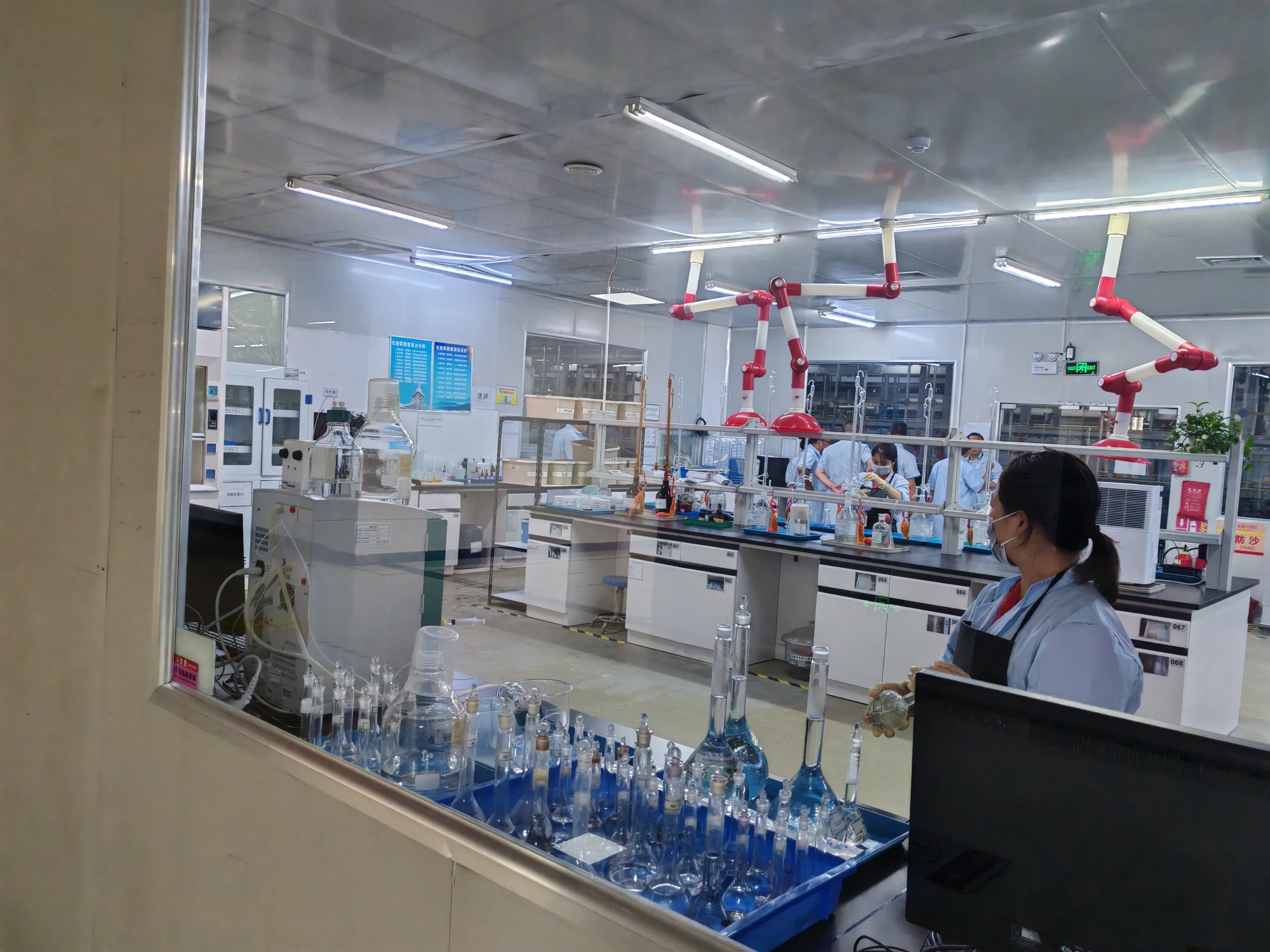
Central Experimental Zone
El UGPCB lab adopts a modular design with the following core areas:
Central Experimental Zone
-
Equipped with corrosion-resistant workbenches surfaced with EPOXY resin to withstand strong acids and alkalis. Glassware such as beakers and measuring cylinders are neatly arranged, and reagent bottles are stored in blue trays by category, implementing 5S management.
Ventilation System
-
Red exhaust ducts connected to multiple fume hoods ensure an airflow speed of 0.5 m/s, keeping organic solvent vapor (p.ej., acetone, isopropyl alcohol) concentrations below occupational exposure limits.
Precision Inspection Zone
-
Configured with a spectrophotometer (for copper ion concentration detection), atomic absorption spectrometer (for heavy metal residue analysis), and XRF coating thickness gauge (accuracy ±0.1 μm). Equipment spacing complies with ISO 14644-1 cleanroom standards.
Core PCB Process Analysis
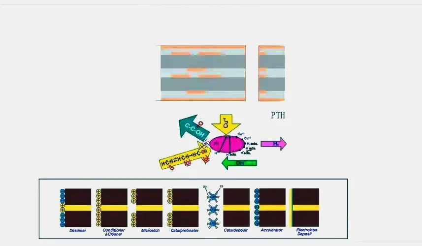
PCB Electroless Copper Plating Process
This process follows a three-stage reaction mechanism:
Pretreatment (Alkaline Potassium Permanganate System)
MnO₄⁻ + H₂O → MnO₂ + 2OH⁻ + O₂↑
Ultrasonic cleaning removes resin residue from tarjeta de circuito impreso hole walls, with roughness controlled to Ra 0.15–0.3 μm.
Activación (Colloidal Palladium System)
Pd²⁺ + Sn²⁺ → Pd-Sn colloidal particles
Ultrasonic assistance ensures uniform catalyst adsorption on microvia (≥0.15 mm) inner walls.
Copper Deposition (Formaldehyde Reduction System)
Cu²⁺ + HCHO + OH⁻ → Cu↓ + HCOO⁻ + H₂O
Parámetros clave: pH 9.0–9.5, temperature 30±0.5°C, deposition rate 2 μm/15 min, copper thickness ≥1.5 μm (per IPC-6012 standard).
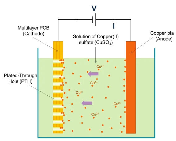
PCB Electroplating Process Optimization
Using a Hull Cell to simulate production conditions, the following reaction ensures plating uniformity:
Anode: Cu → Cu²⁺ + 2e⁻
Cathode: Cu²⁺ + 2e⁻ → Cu↓
Parámetros clave: current density 1.5 A/dm², bath temperature 25±1°C, additive concentration maintained at PCA 5–8 ml/L, ensuring copper thickness deviation on hole walls ≤5%.
Safety and Quality Control System
Lab Safety Protocols
-
Protective Measures: Operators wear nitrile gloves, goggles, and anti-static aprons; face shields are added when handling strong acids.
-
Waste Liquid Treatment: Copper-containing waste is recycled via ion-exchange resin with >60% recovery rate; organic waste is treated with activated carbon adsorption before entering an RTO incineration system.
-
Emergency Management: Equipped with emergency eyewash stations and showers; response time from the nearest fire station is ≤3 minutes.
Real-Time Monitoring System
-
Online Analysis: Conductivity meters monitor impurities in plating baths; automatic pure water replenishment is triggered when Cl⁻ concentration exceeds 50 PPM.
-
Traceability Management: Each batch record includes reagent lot number, equipment calibration date, and operator signature, complying with ISO 17025 lab accreditation requirements.
Industry Applications and Technological Innovation
Comparison of PCB Surface Treatment Processes
| Process Type | Application Scenario | Key Parameters |
|---|---|---|
| ACEPTAR | Interconexión de alta densidad (BGA/CSP) | Nickel thickness 3–5 μm, gold thickness 0.05–0.1 μm |
| OSP | Electrónica de Consumo (Mobile/Tablet) | Film thickness 0.2–0.5 μm, shelf life ≤6 months |
| Inmersión lata | Electrónica automotriz (High-Temperature Resistance) | Tin thickness 1.0±0.2 μm, whisker rate <2% |
Breakthrough Case Study
For a 5G communication board project, UGPCB implemented a dynamic parameter compensation system, logro:
-
30% improvement in microvia copper thickness uniformity (CPK >1.33)
-
Extended electroless copper solution life to 120 m²/L (promedio de la industria: 80 m²/L)
-
100% pass rate in thermal shock testing (288°C × 10s × 3 ciclos)
Conclusión
The UGPCB Chemistry Lab ensures end-to-end quality assurance—from material analysis to final product verification—through precise process control, strict safety management, and continuous technological innovation. Its core technical parameters meet international standards such as IPC-4552A and JPCA-ET01, providing reliable support for high-end applications including 5G base stations, electrónica automotriz, y dispositivos médicos, demonstrating the advanced capabilities of Chinese PCB manufacturing.


