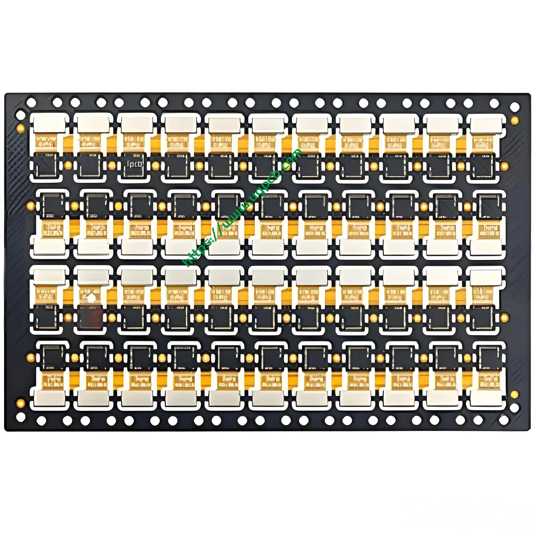
Panoramica del prodotto: The Neural Hub of Mobile Camera Modules
Smartphone camera modules keep getting more complex—multi‑camera, high pixel counts, periscope zoom. Space inside the module becomes extremely tight. Traditional solutions use a rigid PCB plus a separate FPC and a BTB connector. That approach wastes space and risks signal loss or contact failure.
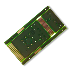
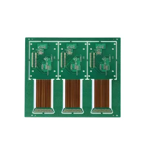
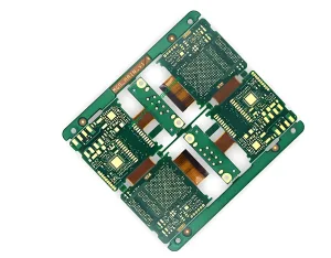
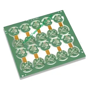
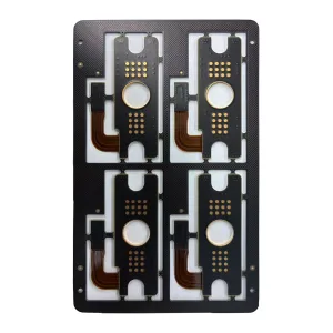
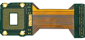
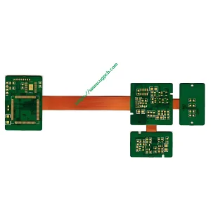
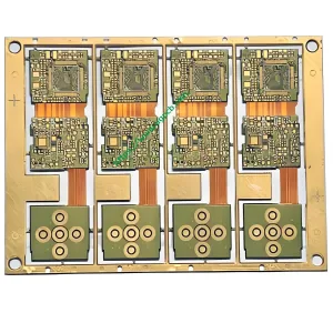
UGPCB solves these problems with our Camera Rigid‑Flex PCB. We integrate rigid and flexible circuit boards into one seamless structure. This board carries the image sensor, autofocus driver, and OIS circuits without any connector.
As a true rigid‑flex PCB, our product combines FR‑4 mechanical strength with polyimide flexibility. UGPCB leverages years of PCB and PCBA manufacturing experience to push precision to new limits. Nostro minimum line width/space is 0.05mm and total thickness is only 0.3mm. These specs perfectly meet the ultra‑thin, high‑density needs of today’s mobile camera modules.
Classificazione & Costruzione: IPC‑6013 Type 4 Precision Build
Classificazione scientifica
We design and manufacture the UGPCB Camera Rigid‑Flex PCB to meet IPC‑6013 Type 4 – Multilayer Rigid‑Flex Printed Board. IPC defines a rigid‑flex board by three features: rigid and flexible materials, three or more conductive layers, and plated through‑holes (PTH). Our product satisfies all three.
Following IPC‑6012 (schede rigide) and IPC‑6013 (flex boards), rigid‑flex boards fall into three categories: rigido, flessibile, and combined. Our product belongs to the third category, designed for mixed assembly.
Multi‑Layer Construction
Our 4‑ to 6‑layer stack‑up uses the following structure:
| Strato | Materiale | Spessore / Spec | Funzione |
|---|---|---|---|
| Rigid zone | FR‑4 glass epoxy | ≈0.2 mm | Carries CMOS sensor, driver IC – provides mechanical support |
| Flexible zone | Poliimide (PI) | ≈0.1 mm | Enables bending inside camera module – supports dynamic flex |
| Copper layers | Lamina di rame elettrolitico | Interno 0.012 mm / Esterno 0.025 mm | High‑density signal routing and power distribution |
| Finitura superficiale | Enepico (Ni/Pd/Au) | Ni 3‑5 μm / Pd 0.05‑0.1 μm / Au 0.03‑0.05 μm | Solderability and aluminum wire bonding |
| Maschera di saldatura | Photoimageable ink | Black or White | Insulation and optical shielding |
The rigid zone uses FR‑4 – the classic rigid PCB material. It offers high mechanical strength and good electrical insulation. The flexible zone uses poliimmide (PI) film. PI has a low CTE (fino a 10 ppm/° C.), excellent flexibility, resistenza al calore, e resistenza chimica. It maintains electrical performance under repeated bending.
We choose 0.012 mm (≈1/3 oz) inner copper to reduce bending stress. IL 0.025 mm (≈2/3 oz) outer copper provides impact strength. For the flexible area, copper thickness stays within 12‑18 μm – proven to balance flex life and electrical performance.
Total finished thickness is only 0.3 mm. Typical rigid‑flex boards measure 0.5‑0.8 mm. Our ultra‑thin design saves more than 50% of Z‑height, giving phone designers valuable space.
Principio di lavoro: Rigid Support + Flexible Interconnect + Seamless Transition
Our rigid‑flex PCB works on three principles:
Rigid zones act as the skeleton – FR‑4 supports the CMOS sensor, autofocus driver, and power management ICs. These components solder onto the rigid surface, forming the module’s brain and heart.
Flexible zones act as joints – PI base material with ultra‑thin copper allows bending at any angle without breaking circuits. The camera module folds into the phone body – for example, bending 90° from the main board to align with the lens opening.
Rigid‑flex transition zones enable seamless connection – Copper traces directly connect rigid and flexible sections during lamination. No connectors, no jumper wires. This eliminates contact resistance, riflessione del segnale, and mechanical loosening. IPC standards note that dielectric changes at the transition can cause impedance fluctuation. UGPCB controls this fluctuation within acceptable limits through precise stack‑up design and impedance tuning.
Specifiche chiave
| Parametro | Valore | Approfondimento tecnico |
|---|---|---|
| Modello | Camera Rigid‑Flex PCB | Dedicated for mobile camera modules |
| Materiale | FR‑4 + PI | FR‑4 for rigid, PI for flexible |
| Conteggio degli strati | 4‑6 layers | Multilayer rigid‑flex construction |
| Colore della maschera di saldatura | Nero / Bianco | Matches optical module requirements |
| Spessore finito | 0.3 mm | Ultra‑thin, saves module space |
| Spessore interno del rame | 0.012 mm (≈1/3 oz) | Reduces bending stress |
| Spessore esterno del rame | 0.025 mm (≈2/3 oz) | Provides mechanical strength |
| Finitura superficiale | Enepico | Compatible with wire bonding and soldering |
| Min line width / spazio | 0.05 mm (2 mil / 2 mil) | Enables high‑density routing |
| Applicazione | Mobile camera modules | Multi‑camera, periscope, foldable phones |
Vantaggi prestazionali: Why UGPCB Stands Out
1. Ultra‑Fine Line Capability – 0.05 mm Line/Space
Our Camera Rigid‑Flex PCB achieves 0.05 mm (2 mil) minimum line width and space. This precision ranks among the industry’s best. Global leaders are pushing toward 40 linee µm, but UGPCB already mass‑produces 50 linee µm.
Why does this matter? A CMOS image sensor (CIS) often has 0.4 mm pin pitch. Finer lines let you fan out more signals in a small area, supporting higher pixel counts and faster frame rates.
When routing on the flexible area of a rigid‑flex PCB, you must keep line width deviation within ≤0.02 mm across the same bend zone. Altrimenti, local stress points cause cracks. UGPCB’s precise etching keeps line width tolerance within ±10% across the entire board, fully compliant with IPC‑A‑600 acceptability requirements.
2. ENEPIG Surface Finish – No More Black Pad
Usiamo Enepico (Elettroless Nickel Electroless Palladium Immersion Gold) as our surface finish. The layer stack is:
-
Nichel (In): 3‑5 μm – diffusion barrier between copper and upper layers
-
Palladio (Pd): 0.05‑0.1 μm – the key innovation that stops Black Pad
-
Oro (Au): 0.03‑0.05 μm – oxidation protection and solderability
The palladium layer completely eliminates the Black Pad defect common with traditional ENIG. Palladium forms a dense film over the nickel, preventing the gold bath from corroding the nickel. This ensures long‑term solder joint reliability.
For camera modules, ENEPIG offers another critical benefit: compatibility with both aluminum wire bonding and soldering. The CMOS sensor chip connects via aluminum wire bonds, while passive components like capacitors need soldering. ENEPIG supports both – a true universal surface finish for rigid‑flex PCBs.
3. 0.3 mm Ultra‑Thin Design – Saves Valuable Space
Inside a smartphone, ogni 0.1 mm counts. Our rigid‑flex board measures just 0.3 mm spessore finito (≈0.2 mm rigid + ≈0.1 mm flex). Compare this to typical rigid PCBs at 0.8‑1.6 mm, or typical rigid‑flex boards at 0.5‑0.8 mm. Our design saves over 50% of thickness. Phone makers can use that space for a thinner body or a larger image sensor.
4. Rigid‑Flex Integration – No Connectors, Higher Reliability
Traditional solutions use three pieces: rigid board + Fpc + BTB connector. This has three big problems:
-
The connector takes up Z‑height
-
Contact resistance (tens of milliohms) causes signal loss
-
Vibration can loosen the connector
UGPCB’s rigid‑flex integration solves all three:
-
Saves over 60% of assembly volume
-
No connector means no contact failure
-
Simplifies assembly – one board does it all
-
Dynamic flex life reaches tens of thousands of cycles thanks to PI and thin copper
5. 4‑6 Layers – Flexible for Any Camera Module
Different camera modules need different complexity:
-
Basic dual‑camera: 4 layers work well
-
Triple or quad‑camera: 6 layers provide enough signal channels
-
Periscope zoom: extra control lines for the zoom mechanism
-
Foldable phone cameras: specially optimized stack‑up for high flex life
UGPCB offers both 4‑layer and 6‑layer configurations. You choose what fits your application.
Linee guida per la progettazione: 5 Key Points for Engineers
1. Bend Area Routing – Follow the Golden Rules (IPC‑2223C)
The flexible zone must endure repeated bending. Follow IPC‑2223C guidelines:
-
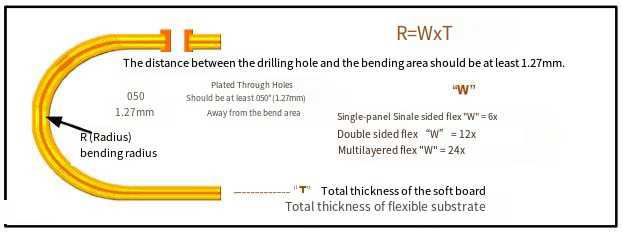
Larghezza della traccia: 0.1‑0.2 mm (4‑8 mil) sull'area flessibile. Evitare 0.05 mm traces there – they increase stress.
-
Routing direction: Route at 45° or 90° to the bend axis. 45° spreads stress; 90° works for dense routing.
-
Minimum bend radius: For dynamic bending, radius ≥ 6‑10 × total flex thickness. Con 0.1 mm flex thickness, raggio minimo ≥ 0.6 mm.
-
No vias or pads in the bend area – they create stress concentration points.
2. Impedance Control – Smooth the Transition
The rigid‑flex transition zone changes the dielectric constant. Impedance can jump by up to 32% if not controlled. UGPCB recommends:
-
Use a gradual line width compensation scheme
-
Make the transition length at least 5× the dielectric thickness
-
Work with UGPCB engineers early – use actual stack‑up parameters for impedance simulation
3. Thermal Management – Copper Thickness and Current
Rigid‑flex boards dissipate heat less effectively than rigid boards. For inner 0.012 mm copper, keep single trace current below 0.3 UN (10°C temperature rise, per IPC‑2221). For power traces, use multiple parallel traces or route on the outer 0.025 mm copper.
4. Material Thermal Matching – CTE Difference
FR‑4 CTE (X/Y) is 13‑18 ppm/°C. PI flex CTE is 25‑35 ppm/°C. The difference exceeds 10 ppm/° C.. This creates stress during reflow. UGPCB controls this by: using low‑CTE PI film (Cte < 10 ppm/° C.), adding a buffer layer at the rigid‑flex interface, and optimizing the reflow profile.
5. Pads and Vias – Use Teardrops and Reinforcement
On rigid‑flex PCBs:
-
Aggiungere teardrop pads where traces meet vias or pads – this increases mechanical strength
-
Coverlay openings should be 0.05‑0.15 mm larger than the pad on each side for reliable soldering
Processo di produzione: 13 Steps from Core to Finished Board
UGPCB follows IPC‑6013 Type 4 Requisiti. The main process steps are:
-
Flex core cutting – High‑quality FCCL (flexible copper clad laminate) cut to size, then plasma treatment (300‑500 W, 60‑90 sec) to increase surface adhesion to Ra 0.4‑0.6 μm.
-
Circuito dello strato interno – Dry film lamination, esposizione, sviluppo, Incisione. Min line 0.05 mm with tight tolerance control.
-
Inner layer AOI – Automatic optical inspection detects opens, pantaloncini, and nicks.
-
Rigid core cutting and inner layer circuit – Same process for FR‑4 cores.
-
Stack‑up and lamination – FR‑4 and PI cores stacked and laminated under high heat and pressure using a stepped pressure profile.
-
Perforazione – Mechanical drilling for PTH holes. Hole diameter tolerance ±0.05 mm.
-
PTH and copper plating – Electroless copper deposition followed by electrolytic plating to reach 0.012 mm (interno) O 0.025 mm (esterno) spessore del rame. Hole wall integrity meets IPC‑A‑600 Class 2/3.
-
Outer layer circuit – Image transfer and etching for final traces.
-
Maschera di saldatura – Black or white photoimageable solder mask applied, esposto, e sviluppato.
-
Surface finish – ENEPIG – Sequential deposition of Ni (3‑5 µm), Pd (0.05‑0.1 μm), e Au (0.03‑0.05 μm).
-
Instradamento / taglio laser – Final shape cut. Rigid zones milled, flexible zones left intact.
-
Prova elettrica & sonda volante - 100% continuity and insulation test.
-
Ispezione finale & packing – Visual inspection per IPC‑A‑600, then vacuum packing.
UGPCB controls layer‑to‑layer registration strictly. Multilayer rigid‑flex boards need registration ≤ ±0.05 mm. Flexible cores can stretch 0.5‑1% during lamination. UGPCB uses a CCD automatic alignment system (positioning accuracy ±0.02 mm) to ensure precise registration.
Scenari di applicazione
Scenario 1: Main Smartphone Camera Module
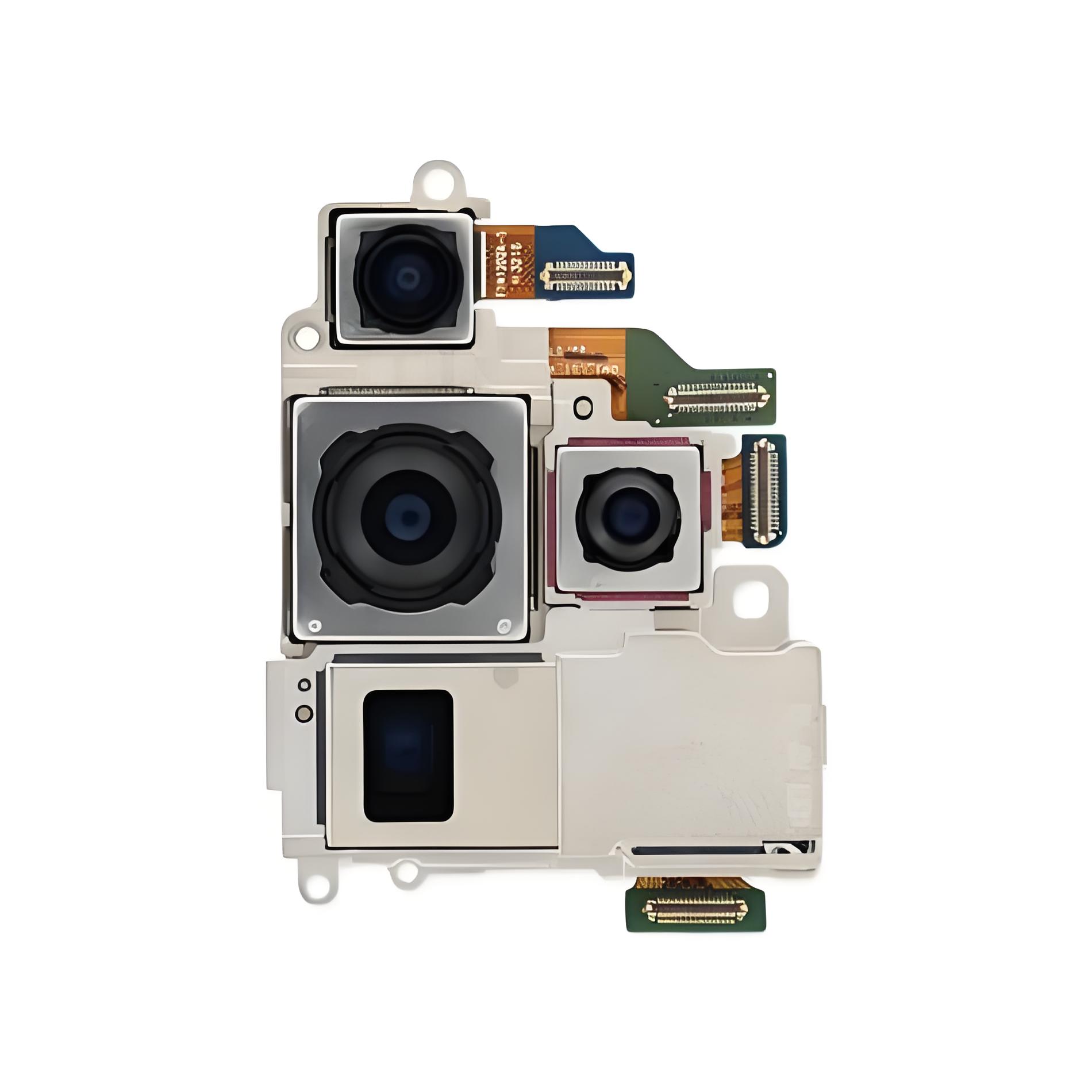
The rear main camera is the largest market for rigid‑flex PCBs. In a typical triple‑camera phone (wide + ultra‑wide + telephoto), our Camera Rigid‑Flex PCB routes all three image sensors to one rigid motherboard, then connects to the phone main board via a BTB connector.
Scenario 2: Periscope Telephoto Module
Periscope modules use a prism to reflect light 90° into a sideways lens assembly. This requires a 90° bend inside the module. Our flexible zone handles that bend easily – no extra FPC or connector.
Scenario 3: Front Camera & Under‑Display Camera
Front camera modules are extremely thickness‑sensitive. Nostro 0.3 mm ultra‑thin rigid‑flex board slips into the narrow gap between the screen and the middle frame. It works especially well for under‑display camera designs.
Scenario 4: Foldable Phone Camera
Foldable phones require dynamic flex life of over 200,000 cicli di piegatura. UGPCB’s PI flexible zone with optimized routing meets this tough requirement.
Scenario 5: Automobilistico & Telecamere di sicurezza
Beyond mobile phones, automotive and security camera modules also need high‑reliability rigid‑flex PCBs. These applications demand more rigorous temperature cycling and vibration tests – for example, 1,000 cycles from -40°C to 125°C per IEC 60068‑2. Our ENEPIG finish and FR‑4+PI material combination meet this reliability level.
Garanzia di qualità: IPC Standards Throughout
UGPCB manufactures and tests Camera Rigid‑Flex PCBs to these international standards:
| Standard | Titolo | Applicazione |
|---|---|---|
| IPC‑6013 Type 4 | Qualification and Performance Specification for Flexible/Rigid‑Flex Printed Boards | Core product standard |
| IPC‑A‑600 | Accettabilità dei circuiti stampati | Visual and structural acceptance |
| IPC‑2221 / IPC‑2223 | Design Standard for Flexible Printed Boards | Design basis |
| IPC‑TM‑650 | Manuale dei metodi di prova | All test methods |
| IEC 60068‑2 | Environmental Testing Series | Temperature cycle, umidità, vibrazione |
| UL 94 V‑0 | Punteggio di infiammabilità | Material fire safety |
UGPCB holds IATF 16949 certificazione di gestione della qualità. Our products comply with RoHS and REACH environmental directives.
The global rigid‑flex PCB market reached approximately $2.604 miliardi di 2025 ed è destinato a crescere fino a $3.726 miliardi di 2032, in un CAGR di 5.25% (fonte: DIResearch). Driven by multi‑camera phones, foldable phones, and automotive cameras, demand for Camera Rigid‑Flex PCBs will keep expanding. UGPCB stands at the forefront of this growth with industry‑leading specifications and a rigorous quality system.
Why Choose UGPCB for Your Camera Rigid‑Flex PCB?
-
✅ Ultra‑fine process capability - 0.05 mm line/space for high‑density camera modules
-
✅ Finitura superficiale ENEPIG – No Black Pad, supports both wire bonding and soldering
-
✅ 0.3 mm ultra‑thin design – Gives you more design space
-
✅ 4‑6 flexible layers – Covers dual‑camera to periscope
-
✅ IPC‑6013 Type 4 certificato – Quality you can trust
-
✅ One‑stop PCBA service – From PCB fabrication to SMT assembly
Get a Quote and Technical Support Now
UGPCB provides complete solutions – from design review and prototyping to volume production and PCBA assembly. Whether you are in the concept stage or have ready‑to‑use Gerber files, our technical team will respond within 24 hours with a professional design review and a fast quote.
📧 Send your inquiry to: sales@ugpcb.com
🌐 Visita il nostro sito web: www.ugpcb.com
📞 Technical support hotline: +86‑755‑2721 1481
Please include the following information for an accurate quote:
-
Conteggio degli strati (4 O 6 strati)
-
Finished dimensions and quantity
-
Colore della maschera di saldatura (nero o bianco)
-
Whether you need PCBA assembly
*Technical data references: IPC‑6013E CN “Qualification and Performance Specification for Flexible/Rigid‑Flex Printed Boards”, IPC‑A‑600H “Accettabilità dei circuiti stampati”, IPC‑2223C “Design Standard for Flexible Printed Boards”, IPC‑TM‑650 “Manuale dei metodi di prova”, IEC 60068‑2 series, DIResearch “Global Rigid‑Flex PCB Market Report 2025‑2032”.*