

 UGPCB 6-Layer Adhesive-Free Rigid-Flex PCB 製品の概要 & 意味
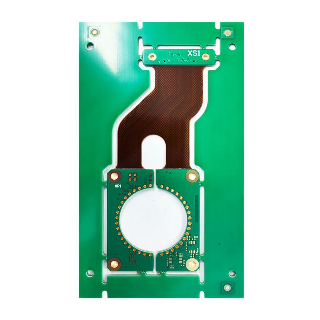
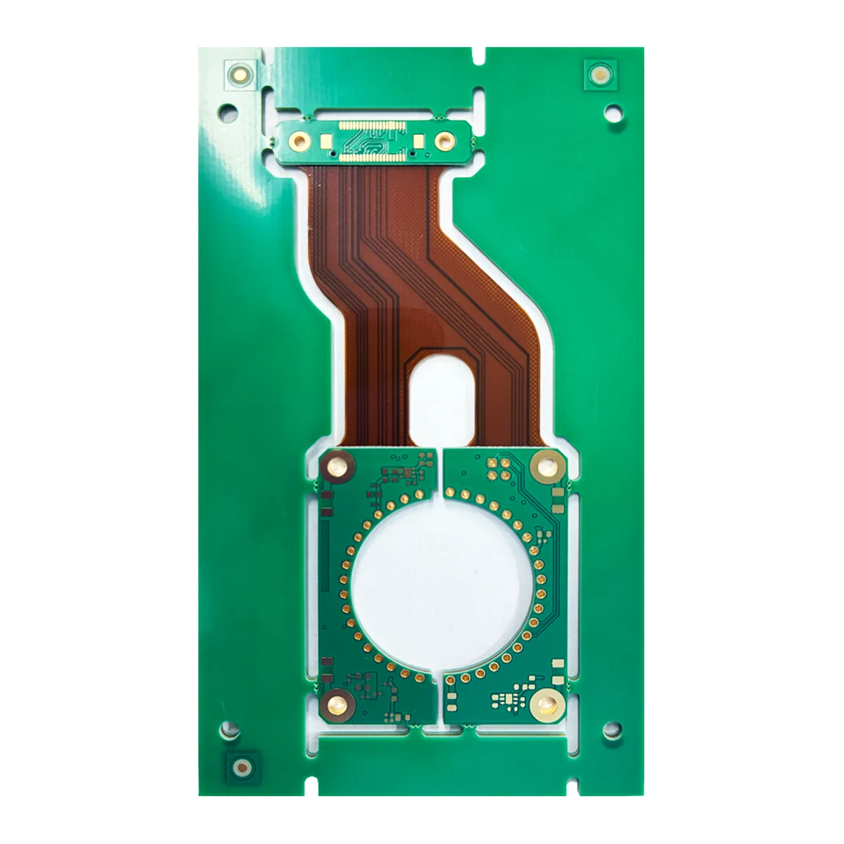
A 6-Layer Rigid-Flex PCB is an advanced プリント基板 technology that integrally combines rigid board stability with flexible circuit dynamic bending capability. This product from UGPCB utilizes a premium adhesive-free lamination プロセス, resulting in a final board thickness of 1.50mm, の寸法 120x80mm, and features an 同意する (エレクトロレスニッケルイマージョンゴールド, 3m”) 表面仕上げ. It represents a cutting-edge solution for 高密度相互接続 (HDI) and three-dimensional electronic packaging, solving complex spatial and mechanical challenges in modern electronics.
科学製品の分類
According to IPC-6013D standards and product construction, this board is accurately classified as:
-
By Construction: Rigid-Flex Printed Board (タイプ 4)
-
レイヤーカウントごとに: Six-Layer Board (combining rigid and flexible layers)
-
テクノロジーによって: Adhesive-less (Adhesive-Free) Flexible Material Rigid-Flex PCB
-
アプリケーションによって: High-Reliability, High-Flex-Cycle Industrial & Medical Grade PCB
Core Structure & 材料
The exceptional performance is rooted in its sophisticated layered structure and top-tier materials:
-
Core Flex Material: 特徴 Shengyi’s 18/50/18 μm adhesive-free double-sided substrate. “18/50/18” denotes a structure of 1 オンス (18μm) 銅 / 50μm Polyimide (PI) dielectric / 1 オンス (18μm) 銅. The adhesive-free construction bonds copper to PI chemically, eliminating adhesive layers, which significantly enhances thermal resistance, 耐薬品性, そして flex circuit 信頼性.
-
Rigid Section Material: 用途 25/25 プリプレグ for lamination in rigid areas, providing robust mechanical support.
-
表面仕上げ: The entire board employs 同意する (3m”). This 3-microinch gold layer offers excellent flatness, 耐酸化性, and solderability for PCB pads, making it ideal for assembling ファインピッチ部品 like BGAs.
Design Key Considerations & 作業原則
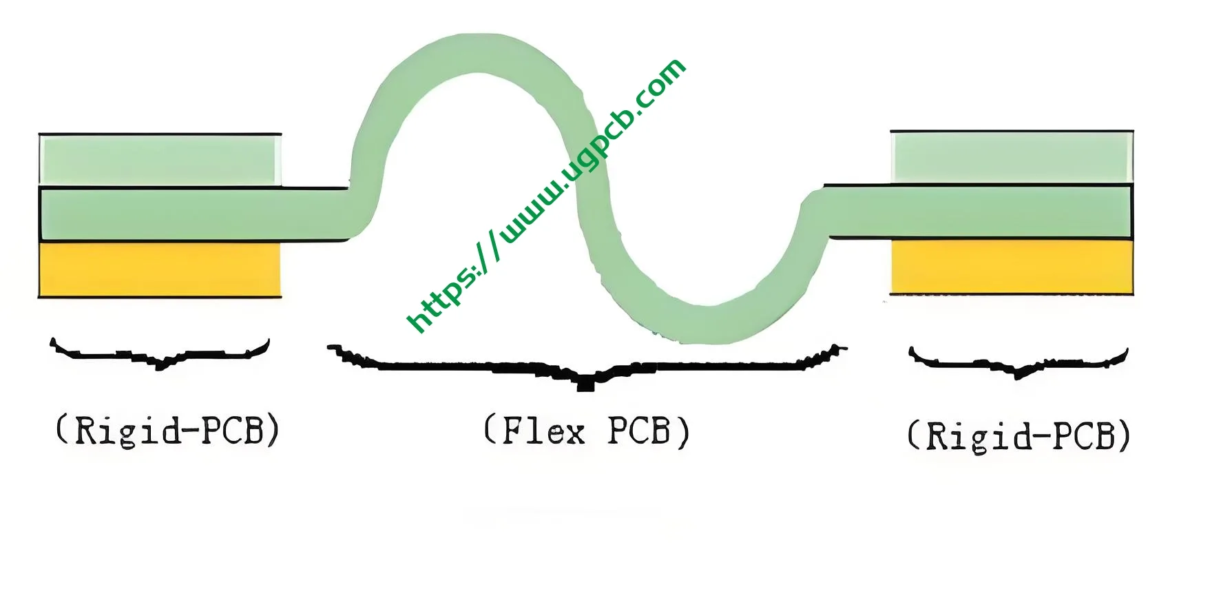
Rigid-flex PCB design is critical for success. The board operates by routing electrical signals through flexible polyimide areas for dynamic movement, while using rigid FR-4 sections for component mounting and structural support.
Essential Design Guidelines Include:
-
Bend Area Definition: Clearly distinguish between static (one-time install) そして dynamic (repeated operation) bend zones. Design the bend radius accordingly. A dynamic bend radius should be at least 10x the flex area thickness (for this board, ≥15mm is recommended).
-
Transition Zone Reinforcement: The rigid-to-flex junction is a stress point. 使用 teardrop pads, curved traces, そして stiffeners to prevent delamination and cracking.
-
インピーダンス制御: For high-speed signals (例えば。, differential pairs) crossing flex areas, precisely calculate trace width and dielectric thickness to maintain consistent 特性インピーダンス (例えば。, 50Ω シングルエンド, 100Ω差動).
-
Flex Routing Rules: In flexible areas, route conductors perpendicular to the bend axis. Use curved or staggered traces to distribute stress evenly.
性能特性 & 利点
Compared to traditional adhesive-based rigid-flex PCBs or rigid-board+connector assemblies, this UGPCB product offers distinct PCB advantages:
-
信頼性の向上: The adhesive-free structure prevents delamination risks from adhesive aging or moisture absorption, increasing flex life by up to 10x and withstands over 100,000 ダイナミックベンドサイクル.
-
Superior Electrical Performance: Uniform PI dielectric with stable dielectric constant (Dk~3.4) ensures signal integrity for high-frequency applications and reduces loss.
-
軽量 & 高密度: Eliminates connectors, ケーブル, and solder joints, enabling 3D assembly. Can reduce system weight by up to 60% and save over 50% 空間.
-
Excellent Durability: Resists extreme temperatures (-55°C〜 +125°C) and chemical exposure, 過酷な環境に適しています.
-
Simplified Assembly: A single integrated component reduces assembly steps, potential failure points, and improves final product yield.
製造工程の概要
UGPCB rigid-flex PCB manufacturing combines advanced rigid PCB fabrication そして flexible circuit production プロセス:
-
内層の製造: Separate etching of rigid FR-4 and flexible PI core layers.
-
ラミネート加工: Precise alignment and high-temperature/pressure bonding of rigid layers, adhesive-free flex cores, and prepreg into a monolithic structure—a critical step in 多層PCB 処理.
-
掘削 & メッキ: Mechanical and laser drilling (if needed) followed by copper deposition and plating to create Plated Through Holes (PTH) for interlayer connection.
-
外層イメージング & エッチング: Pattern formation for outer layer circuits.
-
表面仕上げの塗布: ENIG chemical deposition.
-
Coverlay & プロファイリング: Application of protective film (coverlay) on flex areas. 正確な ルーティング そして レーザー切断 define the board outline and flex section openings.
-
電気試験 & 最終検査: 100% 飛行探査機 or fixture testing for electrical continuity, followed by rigorous visual and dimensional inspection.
主要なアプリケーション & ユースケース
これ 6-layer high-reliability PCB is the ideal choice for demanding applications:
-
航空宇宙 & 防衛: Satellite deployment mechanisms, 誘導システム, avionics sensors requiring utmost reliability and weight reduction.
-
Advanced Medical Devices: 内視鏡, ultrasound probes, wearable monitors needing complex motion and signal transmission in minimal space.
-
Industrial Robotics: Robot joints, internal robotic arm assemblies for seamless power/signal transmission across moving parts.
-
Precision Instruments & 家電: Advanced camera modules, foldable display hinges, drone gimbals pursuing slimness and durability.
-
カーエレクトロニクス: Automated parking sensors, foldable dash displays, in-vehicle camera modules resistant to vibration and thermal cycling.

Ready to integrate superior reliability into your design? Contact UGPCB engineers today for a free design review and quote on your custom 6-Layer Rigid-Flex PCB solution.
 ブラインドビアあり")


 モジュール用")
")


