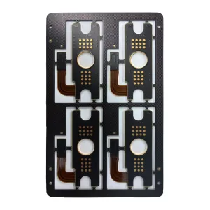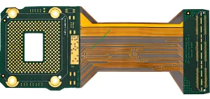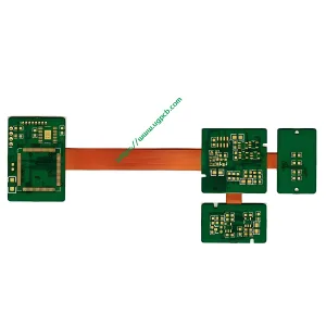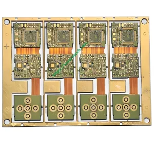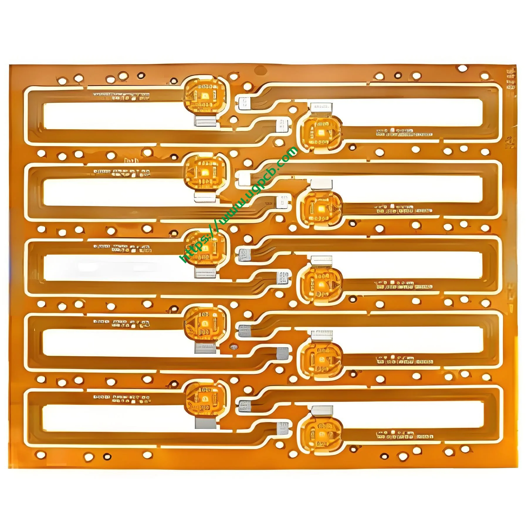
Product Introduction: Fingerprint Identification FPCB – The Critical Carrier in Biometric Era
With the rapid adoption of full-screen smartphones, スマートロック, and keyless car entry systems, fingerprint identification FPCB (Flexible Printed Circuit Board for Fingerprint Identification) has become an essential component in biometric modules. UGPCB leverages over ten years of experience in flexible circuit manufacturing to deliver high-performance fingerprint identification FPC tailored for fingerprint modules. Our products combine precision engineering with stable quality to serve global customers.
This article covers product definition, デザインの必需品, working principle, 材料, 構造, パフォーマンス, manufacturing process, とアプリケーション. It also explains why UGPCB is a reliable partner for your fingerprint identification FPC ニーズ.
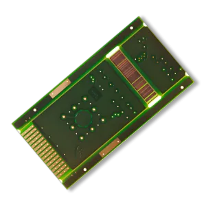
あ fingerprint identification FPCB integrates fingerprint sensing technology with a flexible printed circuit board. Using polyimide (PI) 基材として, it enables high-speed signal transmission between the fingerprint sensor and control chip. Compared to rigid プリント基板, の fingerprint identification FPC is bendable, 超薄型, そして軽量. It fits complex mounting environments such as foldable phone screens, curved covers, and compact mechanical housings.
製品の概要: UGPCB Fingerprint Identification FPCB Key Parameters
UGPCB fingerprint identification FPCB strictly follows IPC-6013 (Qualification and Performance Specification for Flexible Printed Boards). Key parameters are listed below.
| パラメーター | 仕様 | 標準 / 注記 |
|---|---|---|
| モデル | Fingerprint Identification FPCB | UGPCB custom model |
| 基本材料 | ポリイミド (PI) | UL 94 V-0 炎の評価 |
| レイヤー数 | 2 レイヤー | Double-sided board |
| Coverlay Color | 黄色 / 白 | オプション |
| 仕上がり厚さ | 0.15mm | Complies with consumer electronics standard (0.08–0.5mm) |
| 銅の厚さ | 0.5 オズ (18μm) | IPC-6013D tolerance ±12% |
| 表面仕上げ | イマージョンゴールド (同意する) | High wear resistance for fingerprint modules |
Source notes: IPC-6013D では、ベース材料の厚さの許容差 ±8% および銅の厚さの許容差 ±12% を指定しています. UL 94 V-0 内部で自己消火する必要がある 10 数秒で燃え上がる滴りなし. JPCA-ET04 には最小曲げ半径 ≥10T が必要です (T = 総厚さ).
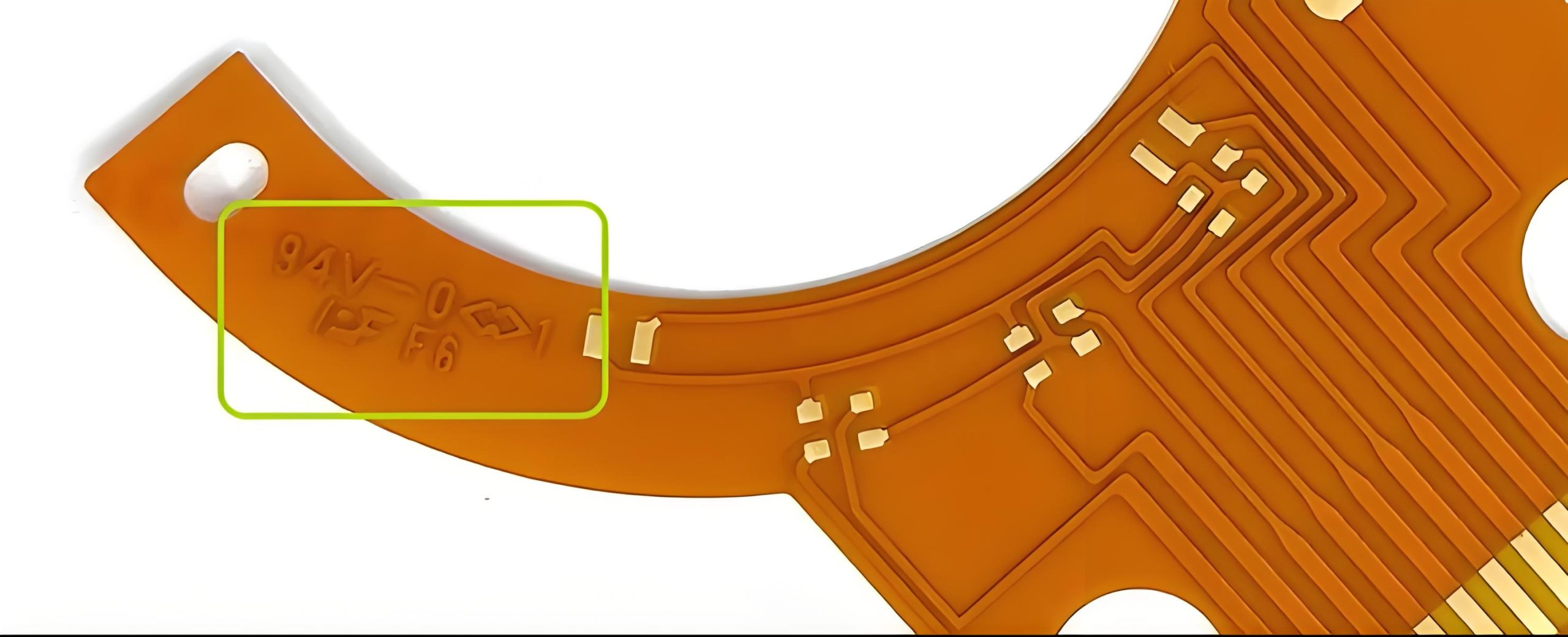
指紋認証 FPCB の定義と科学的分類
意味
あ fingerprint identification FPC 指紋センシング技術を深く統合した特殊なフレキシブル回路基板です. 指紋センサーの電気的接続と機械的サポートを提供します。, ドライバーIC, および信号処理チップ. 信頼性の高い指紋捕捉を保証します, 信号処理, そしてデータ送信.
科学的分類
指紋検知原理に基づく, fingerprint identification FPCB 3 種類のモジュールをサポート:
-
容量性指紋モジュール FPC – 山と谷の間の静電容量の差を利用する. これは家庭用電化製品における主流のソリューションです.
-
Optical Fingerprint Module FPC – Captures fingerprint images using light refraction and reflection.
-
Ultrasonic Fingerprint Module FPC – Uses reflected ultrasound to build 3D fingerprint images. It offers strong penetration and high security.
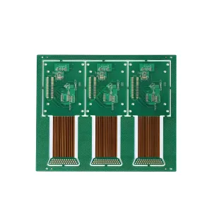
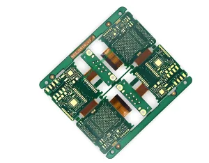
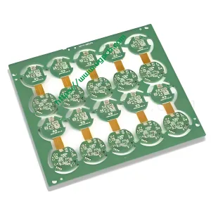
Based on FPC structure, common types include standard double-sided FPC, FPC with raised electrodes, およびリジッドフレックスボード. UGPCB’s 2-layer PI double-sided FPC belongs to the standard double-sided category. It provides high cost-effectiveness, mature processes, and stable performance.
Design Essentials for Fingerprint Identification FPCB
1. Stack-up and Impedance Control
Signal transmission quality directly affects fingerprint recognition speed and accuracy. UGPCB focuses on these key parameters:
-
インピーダンス制御: 50Ω±10% (ref. IPC-2223)
-
Signal loss: <0.3dB/cm @ 40MHz
-
誘電率: PI base material 3.2±0.2 @1GHz
2. Trace Precision and Via Design
-
最小線幅/スペース: 60μm/60μm
-
最小ビア直径: 0.15mm (標準), 0.1mm (ファインピッチ)
-
ビア銅の厚さ: ≧8μm (IPC-6013D準拠)
3. 基板の平坦度
The fingerprint identification FPC 平坦性が必要 <50μm. これにより、センサーと IC の SMT アセンブリ時の同一平面性とはんだ付けの信頼性が保証されます。.
4. 電磁互換性 (EMC) デザイン
指紋モジュールは電磁干渉に敏感です (エミ). UGPCBでは以下のような対策を講じています。:
-
信号層とグランド層間の緊密な結合によりループ面積を最小限に抑える.
-
重要な信号線の周囲にグランド ガード トレースを配置.
-
効果的なESD放電のための補強鋼板の接地抵抗≤1Ω.
指紋認証FPCBの動作原理
例として最も一般的な静電容量式指紋センサーを使用する, の fingerprint identification FPC 4つのステップで動作します.
ステップ 1: 指紋の捕捉. 指がセンサーに触れたとき, 指は一方のコンデンサプレートとして機能し、シリコンセンサーアレイはもう一方のプレートとして機能します。. 尾根 (突起) そして谷 (ギャップ) さまざまな距離を作り出す, したがって、異なる静電容量値. 静電容量センサーはこれらの違いを読み取り、生の指紋信号をキャプチャします。.
ステップ 2: 信号伝送. 生の指紋信号は、 fingerprint identification FPC 信号処理チップへ. FPC の低損失設計により、信号の完全性とノイズ耐性が保証されます。.
ステップ 3: 信号処理とマッチング. 処理チップが強化, 洗練する, 指紋画像から特徴を抽出します. 抽出された特徴を事前に保存された指紋テンプレートと比較します。. 照合アルゴリズムには特徴点ベースの照合が含まれます, テクスチャベースのマッチング, とディープラーニング手法.
ステップ 4: 結果出力. 類似度があらかじめ設定した閾値を超えた場合, システムは認識成功信号を出力します. 今日の主流の静電容量センサーは認識を実現します + 0.15 ~ 0.2 秒のロック解除速度. ユーザーは目立った遅延をほとんど経験しません.
指紋認証用FPCBの材質
基本材料: ポリイミド (PI)
UGPCB はポリイミドを選択 (PI) の絶縁基材として fingerprint identification FPCB. PI には次のような利点があります:
-
高温耐性: SMT アセンブリの場合、260°C を超えるリフローはんだ付けに耐えます.
-
優れた電気絶縁性: 体積抵抗率 >10¹⁶Ω・cm, 高い絶縁耐力.
-
優れた機械的柔軟性: 動的曲げに対する優れた曲げ疲労寿命.
-
炎の評価: UL 94 V-0 準拠 – 内部で自己消火します 10 秒, 燃えるような滴りはありません.
銅箔: 0.5 OZ 圧延焼鈍銅
-
厚さ: 0.5 OZ ≈ 18μm
-
タイプ: 圧延焼鈍銅 – 電着銅よりも優れた柔軟性と耐屈曲性.
-
純度: ≥99.8% Cu
表面仕上げ: イマージョンゴールド (同意する)
-
プロセス: 無電解ニッケル浸漬金 (同意する) – ニッケル層 2~6μm, 金層 ≥0.05μm.
-
利点: 優れた平坦性, 良好なはんだ付け性, 耐酸化性, 耐食性, および複数の挿入サイクル.
-
アプリケーション: 指紋センサー用のワイヤーボンディングとSMTアセンブリ.
指紋認証FPCBの性能
電気性能
| パラメーター | 価値 |
|---|---|
| 絶縁抵抗 | ≥10⁸Ω (正常な状態) |
| 耐電圧 | 500DCで, 1 最小故障なし |
| 導体抵抗 | ≤100Ω/100mm (特定の痕跡) |
| インピーダンス制御 | 50Ω±10% |
機械的性能
| パラメーター | 価値 | 標準 |
|---|---|---|
| 曲げ疲労寿命 | ≥100,000サイクル (R=3mm, 90°曲げる) | - |
| 最小曲げ半径 | ≥10T (T = 総厚さ) | JPCA-ET04 |
| 皮の強度 | ≧0.8kgf/cm | IPC-TM-650 |
環境の信頼性
| テスト項目 | 状態 | 要件 |
|---|---|---|
| 高温保管 | 85℃, 1000h | 水泡なし, 剥離はありません |
| 低温保管 | -40℃, 1000h | 電気的性能は正常 |
| じめじめした暑さ (定常状態) | 85℃/85%RH, 500h | 絶縁抵抗 ≥10⁸ Ω |
| サーマルショック | -40℃ ↔ 85℃, 100 サイクル | オープンなし, 短くない |
| はんだ付け性 | 245℃±5℃, 3–5秒 | 良好な濡れ性 ≥95% |
指紋認証用FPCBの製造工程
UGPCB は IPC-6013 規格に準拠しています. の製造プロセス fingerprint identification FPCB 次の重要な手順が含まれます.
プロセスの概要
Bare FPC fabrication → Solder paste printing → SMT pick-and-place → Reflow soldering → AOI inspection → Component dispensing → Laser cutting & singulation → Underfill → Baking → Metal ring/cover attachment → Pressure baking → Final electrical test → Packaging & 配送
Key Quality Control Points
-
Circuit patterning: LDI laser direct imaging with line width tolerance ±10%.
-
ラミネート加工: Vacuum hot press with pressure fluctuation <5% for good layer adhesion.
-
表面仕上げ: In-line gold thickness monitoring for ENIG – gold layer 0.05–0.1μm.
-
検査: あおい + flying probe test + 4-wire low-resistance test のために 100% electrical yield.
Key SMT Assembly Processes
のために fingerprint identification FPC, special attention is needed during SMT:
-
Stencil design: For BGA fingerprint sensors, use square openings with rounded corners. Area ratio ≥0.66.
-
Reflow profile: Peak temperature 240–250°C, time above 220°C for 60–90 seconds.
-
Placement accuracy: Pick-and-place machine accuracy ±0.05mm for precise chip-to-pad alignment.
Features and Core Advantages
-
Ultra-thin and lightweight: Finished thickness 0.15mm saves valuable internal space.
-
High flexibility: Adapts to curved and folded complex housings. Dynamic bending life exceeds 100,000 サイクル.
-
安定した信号伝送: PI’s low dielectric loss ensures fingerprint signal integrity.
-
高集積化: Supports integration of fingerprint sensor, ドライバーIC, and encryption IC on one board.
-
高い信頼性: ULに会います 94 V-0 flame rating and IPC-6013 performance requirements.
-
優れたはんだ付け性: ENIG surface finish ensures high SMT assembly yield.
Main Applications and Use Scenarios
1. スマートフォン
The fingerprint identification FPC is a core component for under-display fingerprint unlocking and side-mounted fingerprint sensors. In under-display solutions, the FPC connects the fingerprint sensor to the mainboard for high-speed signal transmission. 今日, fingerprint recognition penetration in smartphones exceeds 70%, with under-display as a standard feature in mid-to-high-end models.
2. ラップトップ
Used for user authentication and system login. The fingerprint identification FPC integrates the fingerprint sensor with an encryption chip, enabling fast login, file encryption, and data protection.
3. Smart Locks
In smart locks, の fingerprint identification FPCB must resist water, ほこり, and electrostatic discharge. It ensures long-term stable operation in harsh outdoor environments. 以上 90% of smart locks now include fingerprint recognition.
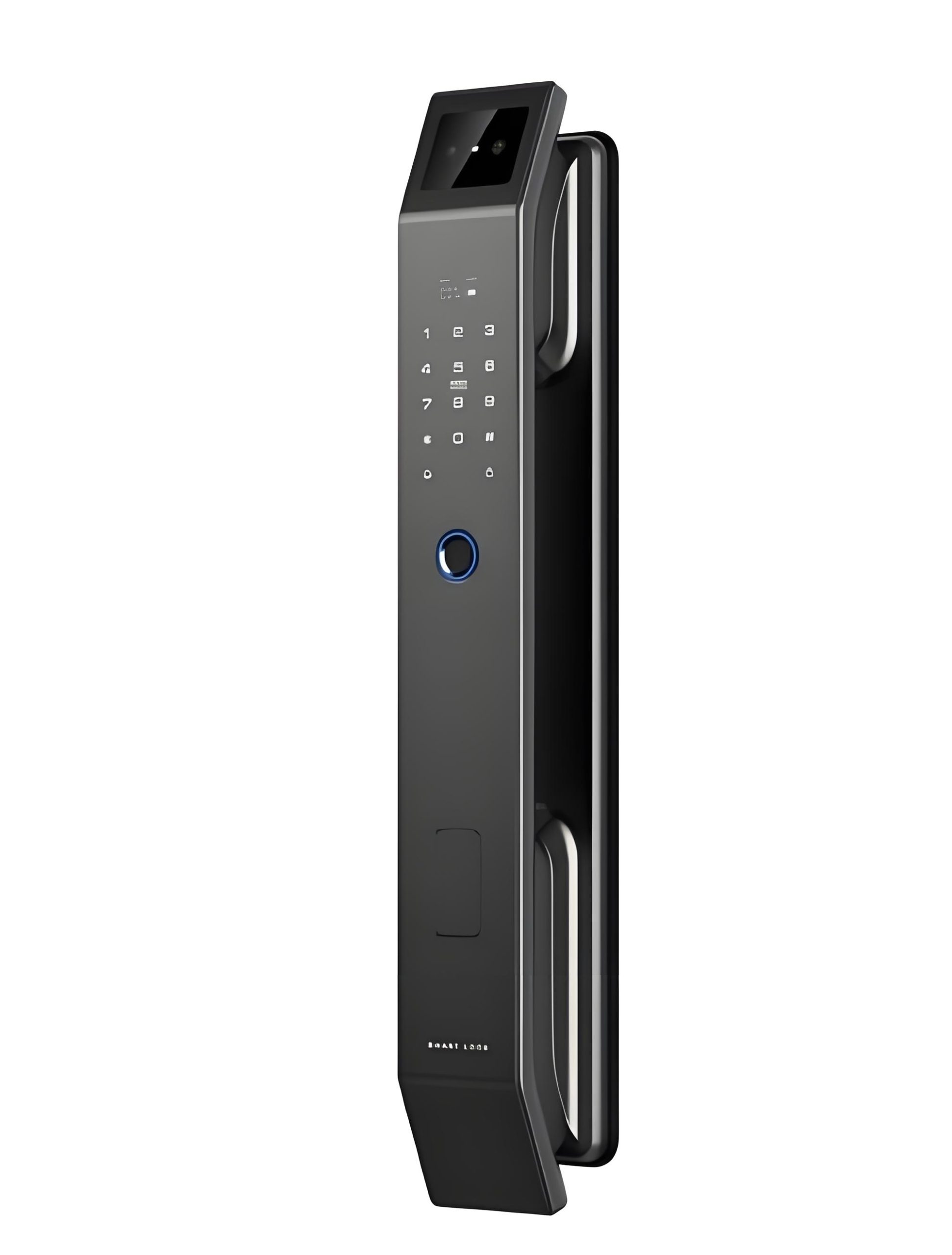
Smart Lock
4. カーエレクトロニクス
Applications include keyless entry systems, start buttons, and steering wheel fingerprint recognition. These systems verify driver identity and improve vehicle security.
5. Financial Payment Terminals
POS システムとセルフサービス金融キオスクの使用 fingerprint identification FPC 支払い確認と取引承認のため.
6. スマートウェアラブル
スマートウォッチとフィットネスバンドには非常にコンパクトで軽量なデザインが必要です. The fingerprint identification FPC これらのデバイスでの高密度統合が可能になります.
市場展望と業界動向
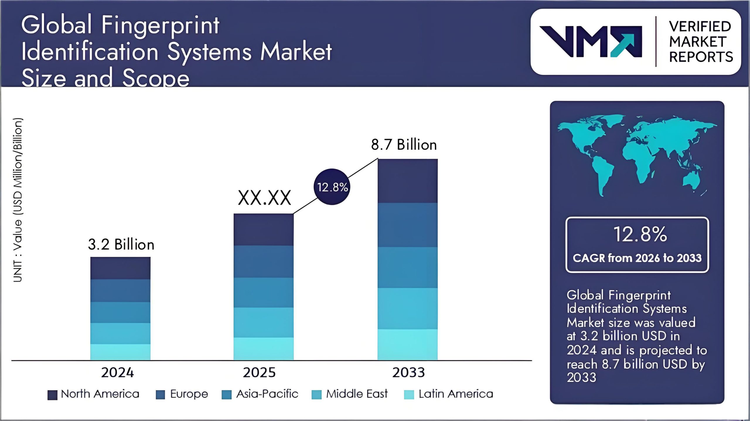
市場調査によると, 世界の容量性指紋モジュール市場は、 $8.857 10億インチ 2025 に $16.290 10億 2031, のcagrで 10.7%. 指紋センサー市場は約 $4.8 10億インチ 2024 に達すると予測されています $8.9 10億 2031, 約のCAGRで 5.50%.
中国では, 指紋認証市場は200億円と推計. 家電製品の割合は約 60%, そしてスマートなセキュリティ (スマートロックを含む) についての説明 25%. スマートロックなどの新興アプリケーション, ウェアラブル, と自動車は指紋認識の第 2 の成長曲線になりつつある.
UGPCB 指紋認証 FPCB を選ぶ理由?
専門的な製造能力
-
10年以上にわたるFPC R&Dおよび製造経験.
-
IPC-6013およびUL規格に完全準拠.
-
100% 電気試験と信頼性検証.
品質保証体制
-
UL 94 V-0 難燃性認定.
-
3段階の品質管理: 受入検査, 工程内制御, そして最終完全検査.
柔軟なカスタマイズサービス
-
色のカスタマイズをサポート, 厚さ, 表面仕上げ, もっと.
-
設計検討からワンストップサービス, プロトタイプのサンプリング, 量産へ.
UGPCB 指紋認証 FPCB のサンプルと見積もりを今すぐ入手してください
UGPCB は高品質の製品を提供することに尽力しています。, 費用対効果 fingerprint identification FPCB 世界中の顧客へ. スマートフォンの指紋モジュールを開発しているかどうか, スマートロックソリューション, または自動車エレクトロニクスプロジェクト, UGPCB はプロフェッショナルなフレキシブル回路基板ソリューションを提供します.
今すぐ行動を起こしてください:
-
📞 技術サポートが必要な場合は、サポート ホットラインにお電話ください。.
-
📧 デザインファイルを当社の営業メールに送信して、迅速な見積もりを取得してください.
-
🌐 UGPCB Web サイトにアクセスしてオンラインでお問い合わせを送信してください.
UGPCB の専門チームが以内に対応します。 24 時間. 私たちはサポートします fingerprint identification FPC サンプルプロトタイピング, 量産, およびカスタムサービス.