
소개: DDR5 PCB 설계의 밀리미터 규모의 전쟁
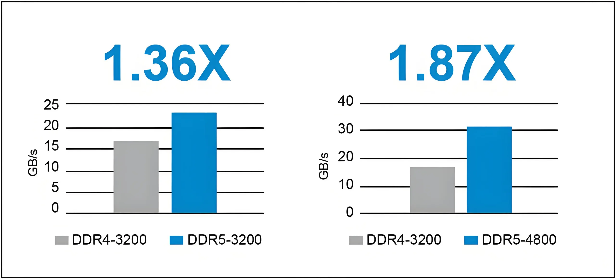
DDR4에서 DDR5로의 도약은 패러다임 전환을 표시합니다.: 신호 속도가 급증합니다 3,200 MT/s to 6,400 MT/S는 작동하는 동안 전압이 1.1V로 급락했습니다. 이 이중 챌린지는 변형됩니다 PCB 간단한 연결 엔지니어링에서 밀리미터 규모의 정밀 전쟁으로 라우팅. 업계 데이터는이를 보여줍니다 80% DDR5 설계 장애는 라우팅 문제에서 비롯됩니다, ~와 함께 90% 층 전 시뮬레이션을 통해 예방할 수 있습니다. 이 기사는 5 가지 중요한 DDR5 라우팅 함정을 해부합니다, 경험적 데이터 및 사례 연구에 의해 뒷받침됩니다, PCB 전문가를위한 실행 가능한 솔루션 제공.
1. DDR5 물리적 특성: 전통적인 PCB 설계 방법이 실패하는 이유
1.1 신호 속도 및 대역폭 혁명
DDR5-6400의 경우, 유효 클록 주파수는 도달합니다 3,200 MHz, 가장 빨리 에지 속도 0.5 추신 (20-80% 상승 시간). 이것은 트리거됩니다:
-
악화 된 피부 효과: 고주파 전류는 도체 표면에 집중합니다, 효과적인 구리 두께 감소 0.66 μm at 10 GHz.
-
유전 손실 에스컬레이션: FR4 기질 손실 접선을 나타냅니다 (Df) ~의 0.02 ~에 10 GHz, 원인 >3 DB/인치 신호 감쇠.
공식 검증 (피부 깊이):

~에 F = 10GHz, Δ≈0.66 μm,전통적인 1oz 구리를 남겨 둡니다 (35 μm) ~와 함께 <2% 이용.
2. 5 개의 DDR5 라우팅 지뢰 및 대책
2.1 지뢰밭 1: 타이밍 오류 - ± 15ps 생존 임계 값
영향: 5 마일 길이의 불일치는 ± 12ps 지연을 도입합니다, 수평 눈 너비가 붕괴됩니다 30%.
사례 연구: GPU 디자인은 BER의 저하를 겪었습니다 10-12 에게 10-7 8mil DQ/DQS SKIC으로 인해.
솔루션:
-
3D 라우팅 보상: 90 °의 평균을 45 ° 세르펜틴으로 교체하십시오, 기생 커패시턴스 감소 30%.
-
동적 타이밍 교정: Monte Carlo 시뮬레이션을 수행하십시오 (케이던스 시그 리티) ± 10% 공정 변화를 다루고 있습니다.
공식 (타이밍 마진):
티여유= t주기- -(티공동+티비행+티지터)
DDR5-6400의 경우 (티주기= 0.3125 ), 시스템 알림이 발생할 때 트리거됩니다 티여유<50 추신.
2.2 지뢰밭 2: 임피던스 불연속성 - 5Ω 신호 쓰나미
위험: 임피던스를 통해 불일치 원인 >15 DB 반환 손실, 수직 안구 높이가 무너지고 40%.
데이터: 추가를 통해 최적화되지 않은 각 0.2 DB 삽입 손실 @5GHz.
솔루션:
-
혁명을 통해: 레이저 맹인 VIA를 구현하십시오 (≤4mil) 안티 파드 보상으로, 임피던스 변화를 ± 3Ω로 제한합니다.
-
패드 최적화: 타원형 패드를 사용하십시오 (1.5:1 종횡비) 용량 성 효과를 줄입니다 20%.
공식 (임피던스 모델을 통해):
Zvia L.87 ⋅ln(5.98시간/(0.8D1+D2))
어디 : 유전체 두께, D1: 직경을 통해, : 패드 직경.
2.3 지뢰밭 3: 크로스 층 지연-0.1ps/mm 나비 효과
섬유 직조 효과: 유전 상수 변화 (Δ .R = 0.3) 유리 섬유 주기성에서 0.6 PS/인치 지연 꼬치.
솔루션:
-
z 축 정렬: 유전체 이방성을 취소하기 위해 ± 45 ° 각도로 바이트 그룹 신호를 경로.
-
크로스 레이어 보상: 자동 지연 보정을위한 EDA 도구로의 기판 DK/DF 데이터 예압.
2.4 지뢰밭 4: 파워 리플 - 1MV 핵 연쇄 반응
감광도: 501.1V 공급의 MV Ripple은 운전자 지터를 증가시킵니다 20%.
시뮬레이션: PDN 대상 임피던스는 기존 디자인보다 100MHz@100 Mhz@≤2 MΩ이어야합니다..
솔루션:
-
3D 커패시터 매트릭스: 0.1μf 배포 (0402) + 10nf (0201) ICS 근처의 커패시터, 피복 10 KHZ – 2GHz.
-
마이크로 코퍼 기둥: BGA에 200μm 직경 기둥을 포함시킨다, 절단 루프 인덕턴스 30%.
2.5 지뢰밭 5: 반환 경로 중단 - 보이지 않는 EMI 폭탄
EMI 위험: 고장난 참조 평면은 공통 모드 노이즈를 생성합니다, EMI 제한을 초과합니다 10 DB.
솔루션:
-
그라운드 스티칭: 그라운드 비아를 배치하십시오 (≤0.1o) 모든 100 신호 레이어 사이의 MIL.
-
분할 비행기 브리징: 묻힌 커패시터를 사용하십시오 (예를 들어, AVX 0402B) 전력 분할을 가로 지르는 10nf 커플 링.
3. DDR5 설계 황금 규칙: 공식 및 공구 체인
3.1 스터브 제한을 통해:DDR5-6400의 경우 (F = 3.2GHz) FR4에서: 그루터기최대≤14.7 mm.

3.2 차동 쌍 내성:
와 함께 티UI= 0.3125 ns 그리고 다섯피= 6 인치/: ΔL≤1.9 mil.

3.3 PDN 임피던스 목표:
50MV 리플 및 10A 과도 전류의 경우: 지목표≤5 MΩ.

4. PCB 설계 프로세스 리엔지니어링: 시험 및 오류에서 시뮬레이션 중심까지
4.1 토폴로지 계획:
-
HFSS의 모델 VIA; 안내서 치수를 최적화하십시오.
-
Siwave를 통해 Stackup 임피던스를 추출하십시오; S-Parameter 라이브러리를 구축하십시오.
4.2 라우팅 실행:
-
Allegro에서 실시간 임피던스 검사를 활성화하십시오; 자동 유체 위반.
-
≤2 mil 그룹 내부 스케일로 플라이 바이 토폴로지를 구현하십시오.
4.3 확인:
-
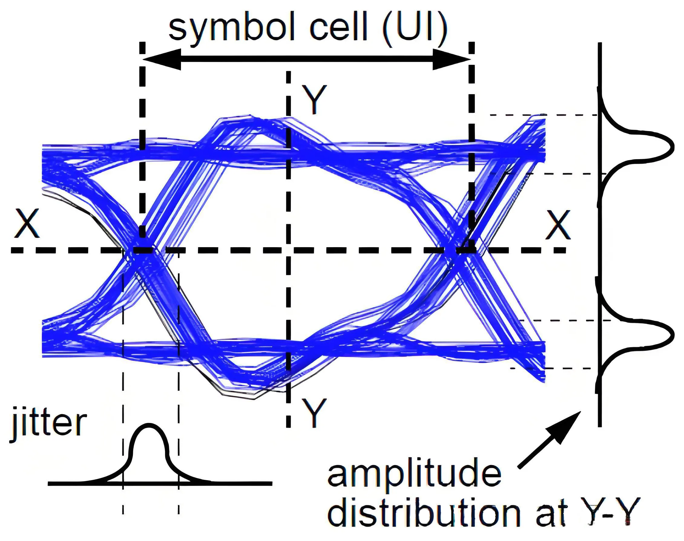
아이 다이어그램 테스트를 수행하십시오 (키 시이트 광고) 70mV 안구 높이 이상.
-
TDR 곡선을 측정하십시오; 임피던스 변동을 ± 5%로 제한.
결론: 그만큼 “세 바디” DDR5 디자인의 법칙
GHZ 속도 아래, 마운드 nuic, 및 미량의 강화 제약 조건, DDR5 PCB 설계는 a “양자 역학” 연대. 신호 무결성 전쟁의 승리는 물질 과학의 수렴을 요구합니다. (저 -DK 기판), 고급 프로세스 (MSAP), 그리고 시뮬레이션 숙달.
