
소개
유연한 인쇄 회로 보드 (FPC) 접이식 스마트 폰에서는 필수 불가능 해졌습니다, 웨어러블 기기, 초대형 프로파일과 구부릴 수있는 특성으로 인한 항공 우주 전자 제품. 하지만, 그들의 디자인 복잡성은 전통적인 견고성을 능가합니다 PCB, 재료 과학에 대한 여러 분야의 전문 지식이 필요합니다, 기계적 시뮬레이션, 프로세스 혁신. 이 포괄적 인 가이드는 융통성의 중요한 측면을 탐구합니다 PCB 설계 업계가 제공하는 방법론과 최첨단 기술을 통해.
1. 재료 과학: 유연한 PCB의 기초
1.1 기판 선택: 성능 및 비용의 균형
유연한 기판은 동시에 열 안정성을 달성해야합니다 (PI의 경우 260 ° C 대 PET의 경우 120 ° C), 굽힘 지구력, 및 유전체 특성. 폴리이미드 (PI) 낮은 CTE로 고급 응용 프로그램을 지배합니다 (≈12 ppm/℃), 폴리 에스테르 동안 (애완 동물) 비용에 민감한 정적 응용 프로그램에 서비스를 제공합니다. 저 모질 루스 PI 기판 (3 gpa) 백만주기 동적 굽힘 내구성을 활성화합니다.
기술 공식:
굽힘 응력 계산:
s = (e · t)/(2아르 자형)
여기서 e = 탄성 계수, t = 두께, r = 굽힘 반경. E를 감소 시키거나 R을 증가 시키면 스트레스 농도가 감소합니다 62%.
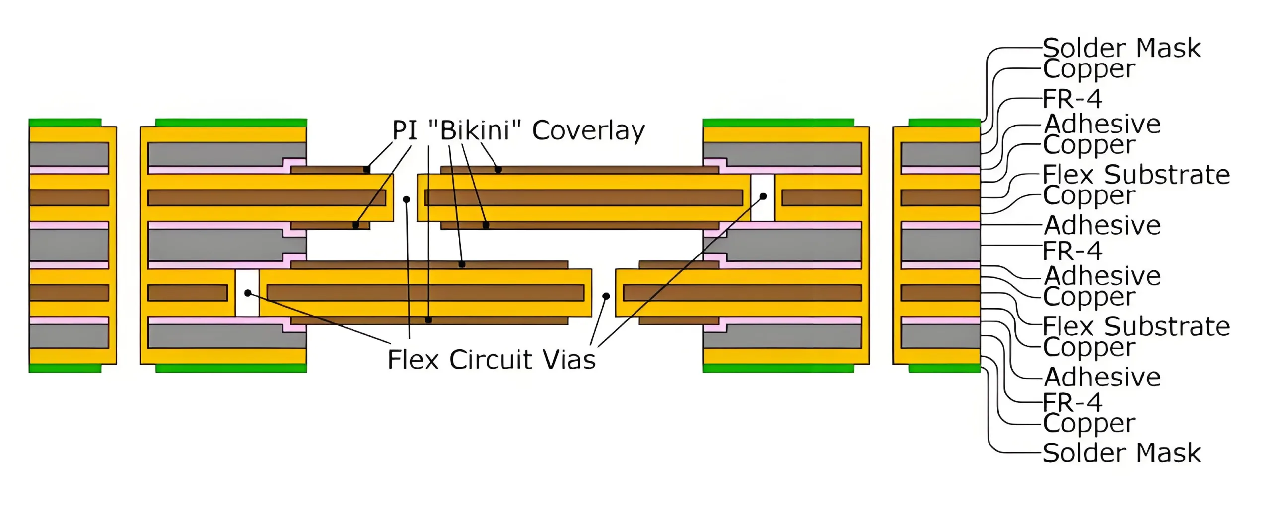
1.2 구리 호일 및 커버 레이: 기계적 조화
롤링 된 매성 (라) 구리 호일은 연성을 향상시킵니다 30% 전극 위에 (에드) 동적 굽힘 영역의 호일. 최적의 CoverLay는 아크릴 접착제를 결합합니다 (15-25μm) 균형 잡힌 접착력 및 유연성을위한 PI 필름.
1.3 보호 계층 혁신
메쉬 그라운드 평면 및 아크 형 구리 강화 (폭이 ≥0.2mm) 분해 위험을 줄입니다 70% 금 손가락과 같은 취약한 지역에서. ENIG 또는 OSP+선택적 금 도금은 신뢰할 수있는 납땜을 보장합니다.
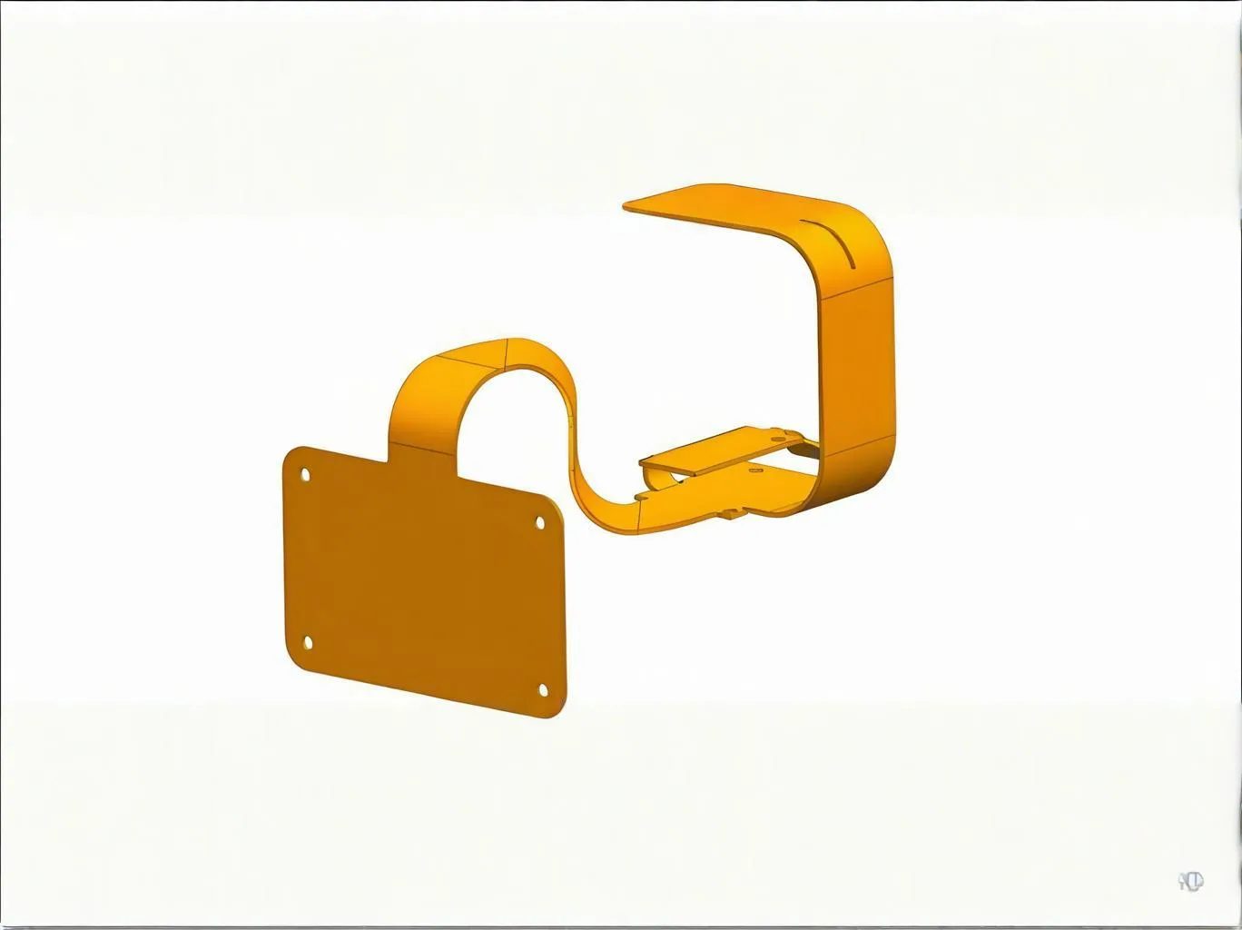
2. 스택 up 아키텍처: 엔지니어링 강성-플렉스 시너지
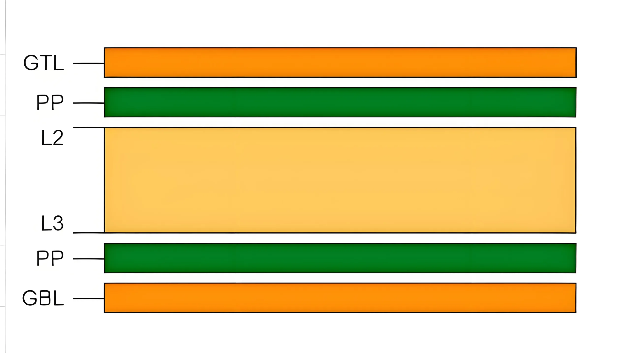
2.1 계층 표준화 및 신호 무결성
-
신호 레이어: 중앙 포지셔닝은 EMI를 최소화합니다
-
발전기: 고체 구리 (50MΩ 목표 임피던스)
-
지상층: 그리드 패턴 (≤5mm 간격) 루프 영역을 줄입니다
사례 연구: 8-2R+4F+2R 구성이있는 Ridid-Flex PCB가 달성됩니다 100,000+ 굽힘주기.
2.2 강성 튀김 전이 구역
수직 라우팅 및 아크 코너가있는 1mm+ 버퍼 영역 구현 (반경 ≥3 × 추적 너비) 스트레스를 분배합니다.
3. 동적 굽힘 최적화
3.1 반경 골든 규칙을 구부리십시오
최소 굽힘 반경 요구 사항:
-
공전: 아르 자형<보결>분</보결> ≥5T
-
동적: 아르 자형<보결>분</보결> ≥10t
(예를 들어, 0.2MM PI는 ≥2mm 동적 반경이 필요합니다)
3.2 시뮬레이션 중심 검증
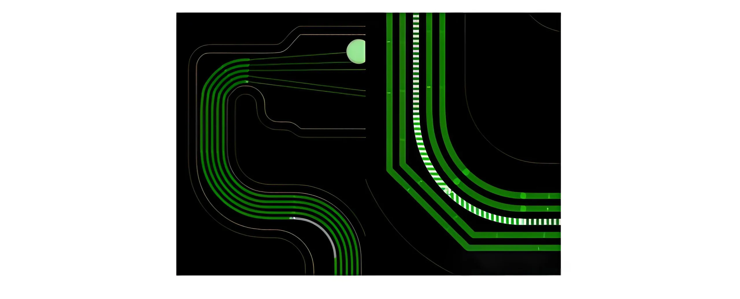
유한 요소 분석 (fea) 고갈 영역을 식별합니다. 접이식 전화의 뱀 라우팅은 피로 수명을 향상시킵니다 200,000+ 사이클.
4. 라우팅 원리: 전기 기계적 균형
4.1 굽힘 영역 금지
-
벤드 라인 5mm 이내에 VIAS/구성 요소가 없습니다
-
비틀 거리는 인접한 층 흔적은 방지합니다 “I- 빔” 스트레스
4.2 임피던스 제어
고속 신호에 대한 특징적인 임피던스 공식:
z₀ = [87/√(이자형<보결>아르 자형</보결>+1.41)] × LN[5.98시간/(0.8w+t)]
그 중, 이자형아르 자형 유전체 상수입니다, H는 유전체 두께입니다, w는 선 너비입니다, 그리고 T는 구리 두께입니다.
차동 뱀 라우팅 (2× 간격) Crosstalk를 최소화합니다.
5. 제조 협업
5.1 IPC-2581 표준 구현
통합 XML 형식은 통신 오류를 줄입니다 80%, 첫 번째 통과 수익률 향상 65% 에게 92% 드론 안테나 프로젝트에서.
5.2 DFM 지침
-
추적 간격: ≥4mil
-
레이저 드릴링: ≥4mil 구멍 (± 1mil 정확도)
-
커버 레이 오프닝: 0.1패드보다 큰 mm
6. 미래의 프론티어
6.1 3D 신축성 회로
UESTC의 3D-LSC 프로세스는 5 층 스택으로 미터 규모의 플렉스 회로를 가능하게합니다., 의료 웨어러블에 적용됩니다.
6.2 나노 물질 혁신
그래 핀/PU 복합재가 달성됩니다 10<한모금>-6</한모금> ω · 100k 구부러진 후 5% 성능 저하로 CM 저항성.
결론
유연한 PCB 디자인 재료의 학제 간 혁신을 요구합니다, 역학, 그리고 전자 장치. 이러한 전략을 구현하고 IPC-2581과 같은 새로운 표준을 채택함으로써, 엔지니어는 고급 응용 프로그램에 대한 신뢰성과 밀도로 차세대 플렉스 회로를 개발할 수 있습니다..
