
조용한 재료 혁명은 전자 제품을 재구성합니다
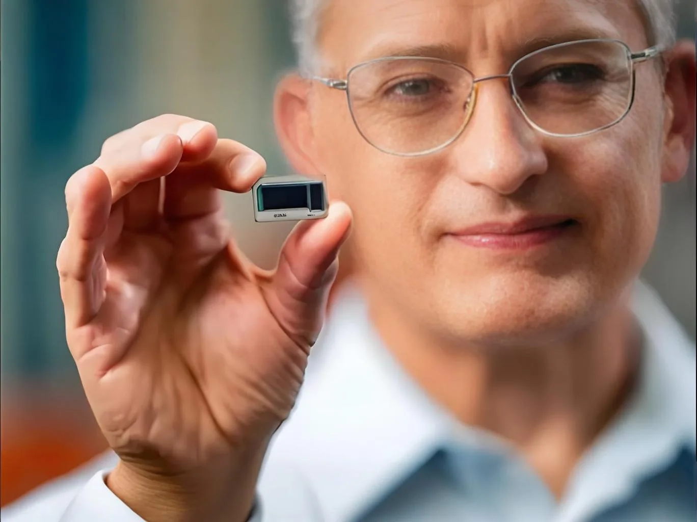
인텔 2024 글로벌 데뷔 유리 기판 포장 기술은 반도체 제조의 지진 변화를 폭발시켰다. 에서 2025 Suzhou TGV 산업 정상 회담, 인텔의 기술 리더, TSMC, 삼성은 동의했다: “유리 기판은 반도체 포장을 '투명한 시대로 유도합니다.,’ 시장 침투가 초과되었습니다 50% 5 년 안에.” 이 분석은 기술적 근거를 탐구합니다, 산업 체인 변환, 그리고에 대한 의미 PCB 산업.
1. 기술적 우월성: 유리 기판이 포장을 재정의하는 이유
1.1 물리적 재산 지배
비교 분석은 유리 기판을 보여줍니다’ 압도적 인 장점 :
| 매개 변수 | 유기 기판 | 실리콘 개입 | 유리 기판 |
|---|---|---|---|
| 유전 상수 | 4.2-4.8 | 11.9 | 3.9 |
| 손실 탄젠트 | 0.02-0.04 | 0.001-0.01 | 0.0001-0.001 |
| CTE (ppm/°C) | 16-18 | 2.6 | 3.2-7.5 (조정할 수 있는) |
| 열전도율 | 0.2-0.3 | 150 | 1.1 |
| 표면 거칠기 | 0.5-1.0 μm | 0.05 μm | <0.01 μm |
(원천: 인텔 기술 백서, 코닝 재료 연구소)
신호 손실 방정식 분석
감쇠 (에이) 정의됩니다:

ε'≈3.9 및 ε”유리 기판의 경우 ≈0.001, 고주파 (100GHz) 손실은 감소합니다 67% 유기 기질 대 (E'4.5, 이자형”≈0.03).
1.2 지수 밀도 향상
NVIDIA의 GB200 GPU가 시연합니다 50%+ 유리 기판을 사용하여 다이 카운트 증가, 5μm/5μm 배선 밀도를 달성합니다:
-
원자 수준의 평탄도 (<0.01μM 거칠기)
-
조정 가능한 CTE 매칭 (3ppm/°C)
-
기계적 안정성 (700× 700mm 패널 warpage <50μm)
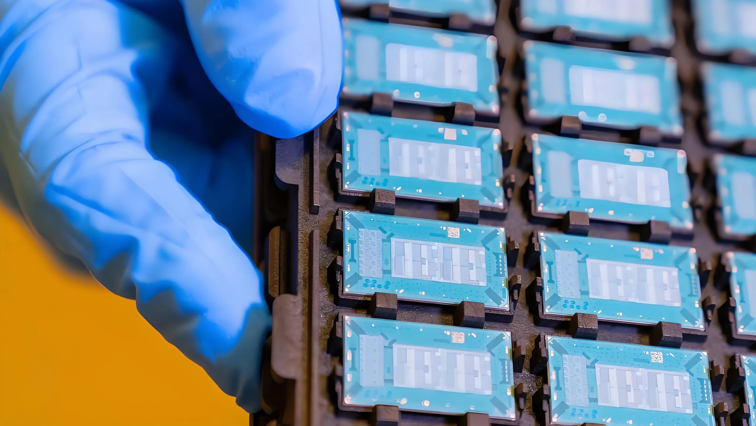
2. 프로세스 혁신: TGV 기술 산업화
2.1 유리-비아 제조 혁신
Titanrise Tech의 레이저 수정이 달성됩니다 8,000 vias/sec ± 5μm 정밀도 (3에이), 160× 기존 방법보다 빠릅니다. 주요 단계:
-
피코 초 레이저 수정: 미세 스케일 변경 구역을 만듭니다
-
HF 에칭: 달성 100:1 종횡비
-
금속 화: PVD 스퍼터링 + 전기 도금 (>15MPA 접착력)
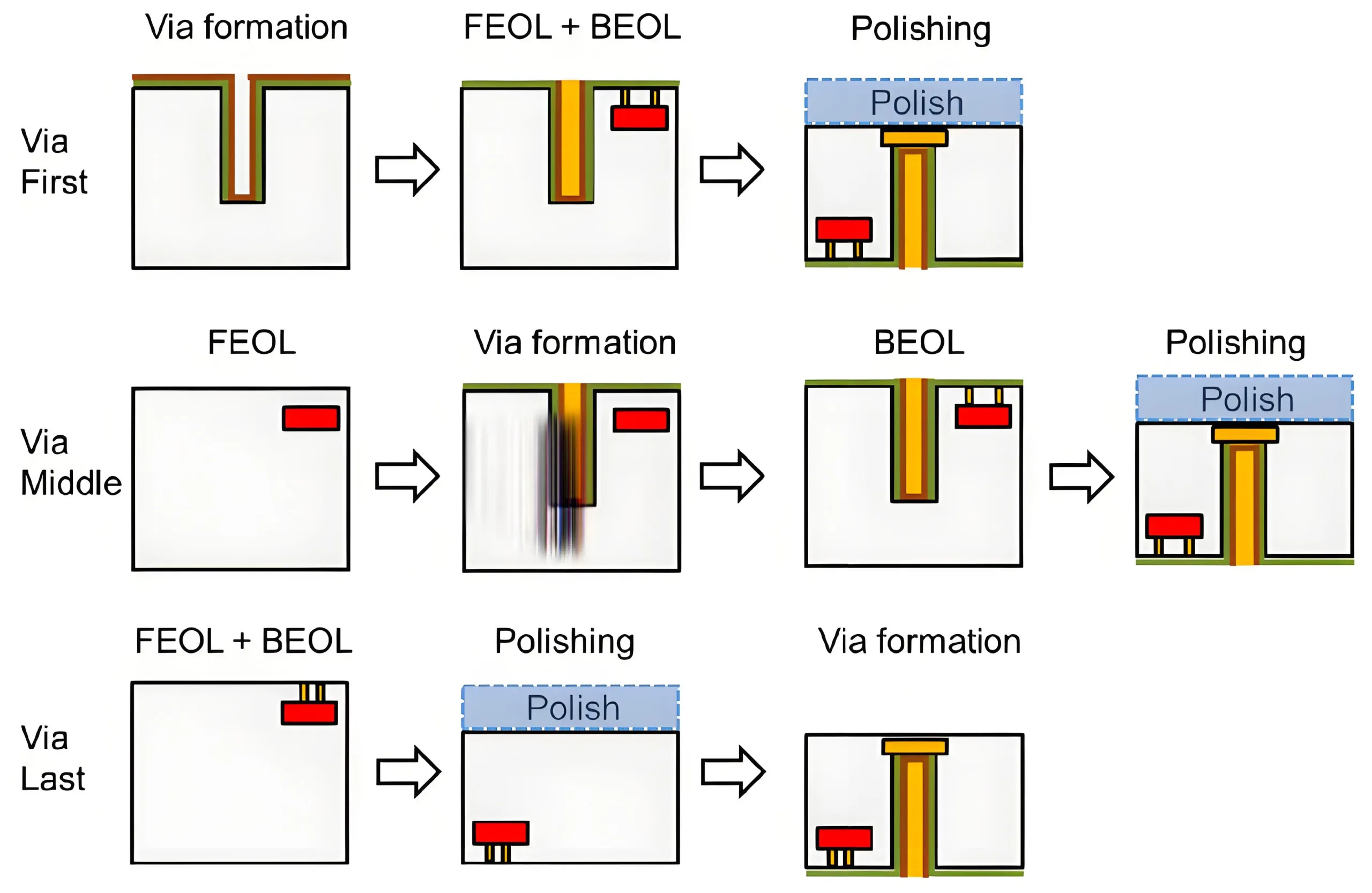
2.2 금속화 발전
4 개의 기술 경로는 유리 접착력을 다루고 있습니다:
-
전자식 + 마이크로 에칭 (AKM 솔루션)
-
나노 AG 페이스트 + LT 소결 (Wintech 특허)
-
혈장 이식 (IME-CAS 기술)
-
PVD TI/스택 (Titanrise 표준)
그 중, UGPCB DEP600 장비를 도입하는 데 많은 투자를했습니다, 높은 종횡비 스퍼터링 기술을 채택합니다, 달성 95% 적용 범위 10:1 홀 프로파일, 금속 저항력이 적습니다 2.5 μΩ · cm, 국제적으로 선도적 인 수준에 도달합니다.
3. 산업 환경: 글로벌 경쟁이 강화됩니다
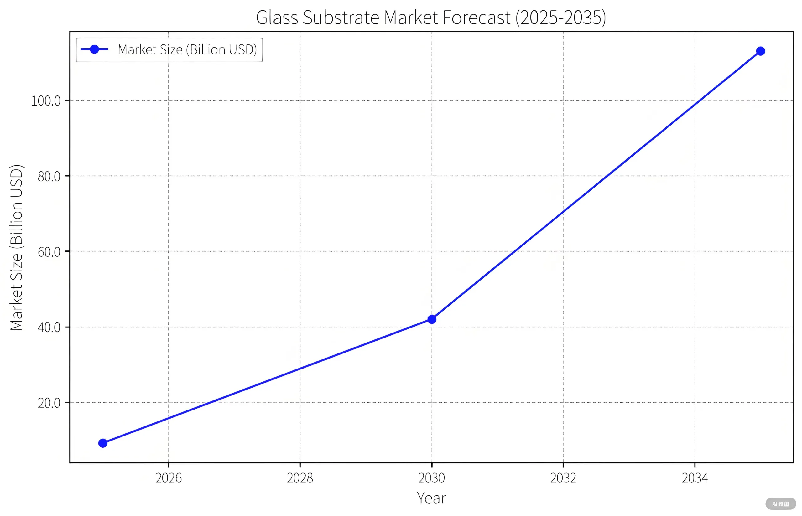
3.1 시장 성장 예측
Prismark는 폭발성 확장을 예측합니다:
-
2025: $916중 (TGV 기질)
-
2030: $4.2비 (전체 응용 프로그램)
-
2035: $11.3비 (전체 생태계)
3.2 지정 학적 기술 경주
-
미국: 인텔 표준 + 코닝 공급 지배
-
한국: 삼성 “유리 동맹” + SKC의 9 층 스택
-
중국: Wintech/AKM 대량 생산 + JFE 2026 현지화
4. 도전 & 솔루션: 상업화 장애물
4.1 비용 절감 경로
현재 3-5 × 비용 프리미엄 대 전통적인 기판이 급락합니다.:
-
85% 큰 패널 (>2m²) 이용
-
90% 레이저 드릴링 비용 절감
-
금속화 수율 개선 (60%→ 92%)
4.2 신뢰성 인증
새로운 표준이 필요합니다:
-
열 사이클링 (-55° C – 250 ° C, 1,000 사이클)
-
평생 (MTTF >10시간 @ JEP154 시간)
-
고주파 안정성 (<0.5DB/CM @100GHz)
5. PCB 산업적 영향: 위협 대 기회
5.1 시장 혼란
-
30% HDI/기판 교체 위험
-
잡종 (유리+수지) 기판 기회
5.2 기술 시너지
-
피코 초 레이저 드릴링 채택
-
PVD 강화 HDI 추적 정밀도
-
광학 검사 <0.1μM 분해능
결론: 투명한 기판, 불투명 미래
중국은 현재 중요한 TGV 부문을 이끌고 있습니다 (장비, 테스트, 재료). 인텔의 Pat Gelsinger가 지적한 것처럼: “재료 혁신은 원자 규모에서 새로운 무어의 법칙이됩니다.” 이 유리 중심 혁명은 반도체의 두 번째 성장 곡선을 잠금 해제 할 수 있습니다.
