
BGA 솔더 패드의 단지 0.5mm² 균열은 프리미엄 스마트 폰을 “흰색 스크린 서류” - 기존의 언더 필 캡슐화는이 중요한 PCB 신뢰성 위협을 위장합니다.. 스마트 폰이 매우 얇은 디자인 및 고성능 사양으로 빠르게 발전함에 따라, BGA 패드 크래킹 Damocles가되었습니다’ 칼이 매달려 있습니다 PCB 조작. 언제 a $1,000+ 휴대 전화 PCB 조립 마이크로 크랙 또는 시장 수익률 급증으로 인해 스크랩이됩니다. 30% ~에서 타입 V 골절, 우리는 물어봐야합니다: 진정으로 궁극적 인 해결책입니다?
1. BGA 패드 크래킹: 전자 제품의 보이지 않는 살인자
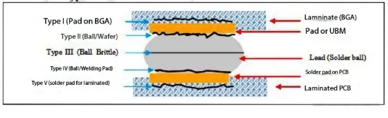
H3: 1.1 실패 정의 & 5 가지 골절 유형
BGA 패드 크래킹 사이의 분리를 나타냅니다 IC 칩 기계적/열 응력 하에서 PCB 패드. 5 가지 골절 유형은 위치별로 분류됩니다:
| 유형 | 실패 위치 | 널리 퍼짐 | 기본 트리거 |
|---|---|---|---|
| I 형 I | 칩 기판 층 | 12% | 텀블링 테스트, 기계적 충격 |
| II 형 | BGA PAD-SOLDER 인터페이스 | 18% | 열 사이클링 |
| III 형 | 무연 솔더 볼 | 25% | 낙하 충격, 열 충격 |
| IV 형 | 솔더 PCB 패드 조인트 | 28% | 리플 로우 프로파일 불일치 |
| 타입 V. | PAD-SUBSTRATE 분리 | 17% | 구조적 변형, 재료 저하 |
1.2 스텔스 본성 & 파괴적인 영향
전통적인 SMT 검사가 감지됩니다 <5% 그로 인한 패드 균열:
-
마이크로 크랙 크기 (5-50μm) 다층 PCB에 가려졌습니다
-
전기 연속성은 종종 골절에도 불구하고 유지됩니다
-
언더필은 전파를 중단하지 않고 균열을 마스크합니다, 재 작업 중에는 파괴적인 제거가 필요합니다

2. PCBA 워크 플로의 근본 원인 분석
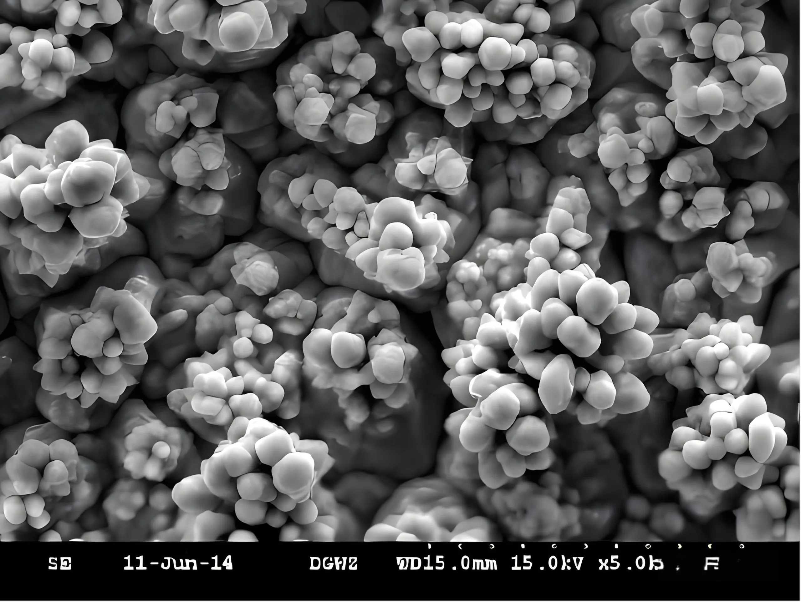
2.1 재료 기원: 구리 포일 결정 구조 발산
실험 데이터가 드러납니다: 전문화 된 구리 호일 “포도 같은” 결절 구조가 제공됩니다 18.5% 기존 결정보다 높은 접착력.
2.2 PCB 기판 제한: FR4의 열 지구력 위기
무연 납땜은 248 ° C의 최대 온도를 요구합니다 (+33° C 대 전통적인 프로세스). 표준 FR4 130-140 ° C의 TG 원인:
-
z 축 Cte >300 ppm/°C
-
T288 박리 시간 <3 분 (산업이 필요합니다 >5 분)
중요한 공식: 열 응력 = E × α × ΔT
어디:
σ = 열 응력 (MPA), E = 탄성 계수 (GPA),
α = CTE (ppm/°C), ΔT = 온도 변화 (℃)
*고 CTE 기판은 ΔT = 100 ° C에서 1.8 × 더 많은 응력을 생성합니다.
2.3 PCB 설계 함정: 간과 된 기계적 스트레스
분석 7,000 러시아 시장에서 실패한 단위가 보여줍니다:
-
0.80MM 보드는 1.00mm 이상 3.2 × 이상 실패했습니다
-
T- 카드 슬롯은 PCBA 크래킹 위험을 증가시켰다 47%
-
BGA 영역 하의 큰 구성 요소는 비대칭 열 변형을 일으켰습니다
3. 중요한 PCB 프로세스 제어 혁신
3.1 PCB 제조 최적화 매트릭스
| 프로세스 | 전통적인 | 최적화 | 개선 |
|---|---|---|---|
| 구리 호일 | 표준 결절 | 포도 같은 결정 | 접착력 ↑ 18.5% |
| 도금 두께 | 18-23μm | ≥30μm | 인장 ↑ 32% |
| 표면 준비 | 벨트 샌딩 | 마이크로 에칭 + 스프레이 | 구리 손실 ↓ 60% |
| 솔더 마스크 개구부 | 회보 | 육각형 | 페이스트 흐름 ↑ 40% |
3.2 리플 로우 프로파일 혁명
실패 루트: 표준 리플 로우는 190 ° C → 130 ° C에서 12 초만 냉각됩니다, 빠른 수축을 유발합니다.
해결책: tg 이상으로 거주 시간을 연장합니다 150%, 열 응력 감소 35%.
4. 포괄적 인 PCBA 솔루션 데이터베이스
4.1 디자인 혁신
-
패드 형상: 말초 패드를 타원형으로 변환하십시오 (장축 +0.1mm)
-
스택 업 디자인: BGA 아래에 현지화 된 구리 균형 층을 추가하십시오
-
통관 규칙: 큰 금지 구성 요소 BGA 영역에서 3mm 이내
4.2 자재 업그레이드 경로
-
TG ≥170 ° C로 FR4를 지정하십시오
-
구리 포일 Rz를 제어합니다 (거) 3.5-5.0μm에서
-
로우 CTE를 채택하십시오 (<2.5%) 하이-가공 수지 시스템
4.3 프로세스 제어 레드 라인
-
구리 도금 ≥30μm (검증되었습니다)
-
OSP 패널 간격 >5mm (산 포획 방지)
-
시험 고정 압력 ≤7kg/cm², 핀 라이프 <500K 사이클
-
150-180° C 반사 구역은 ≥90 초입니다
5. 미래의 기술 로드맵
처럼 HDI PCB 0.4mm 두께로 전진하고 BGA 패드는 0.2mm 미만으로 줄어 듭니다., 돌파구가 필요합니다:
-
나노 규모의 구리 처리: 마그네트론 스퍼터링 된 접착 층
-
CTE 조용 기질: 온도-반응성 중합체 복합재
-
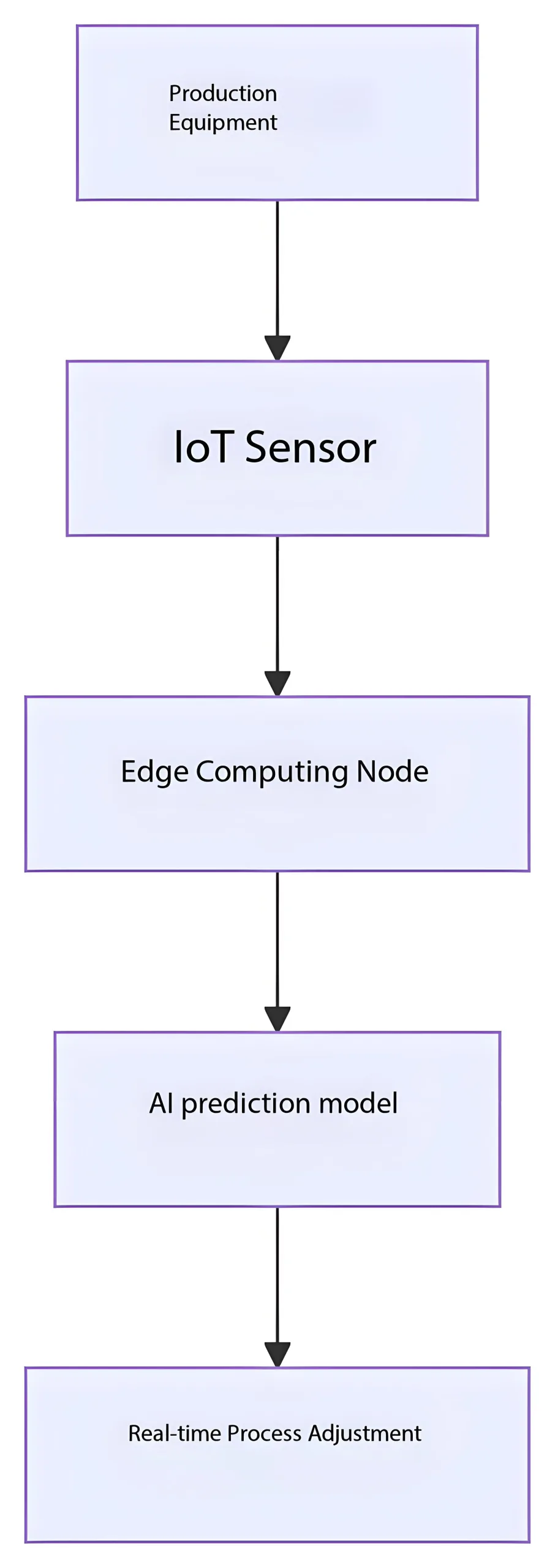
AI 프로세스 모니터링: 실시간 솔더 공동 건강 예측
결론: 신뢰성은 설계되었습니다
BGA 패드 크래킹이 구성됩니다 시스템 수준 신뢰성 실패. 구현 후 결과:
-
텀블링 테스트 패스율: 82% → 99.6%
-
시장 수익률: ↓ 70%
-
비용 절감: $1.20/Underfill 제거를 통한 보드
*기억하다: PAD 당 접착력의 0.1KGF 증가는 지수 신뢰성 이익을 제공합니다.. 이것은 프로세스 정제를 초월합니다-그것은 제로 결함 제조의 궁극적 인 추구를 구현합니다.*.
솔더 패드의 미세한 영역에서, 포도와 같은 구리 결정은 나노 스케일 보호 네트워크를 짜냅니다, 무연 구체는 육각 마스크 개구부 내에서 정밀 댄스를 수행하는 동안. 전자 제품 신뢰성 혁명은 0.01mm마다 흔들리지 않는 헌신으로 시작합니다..
