

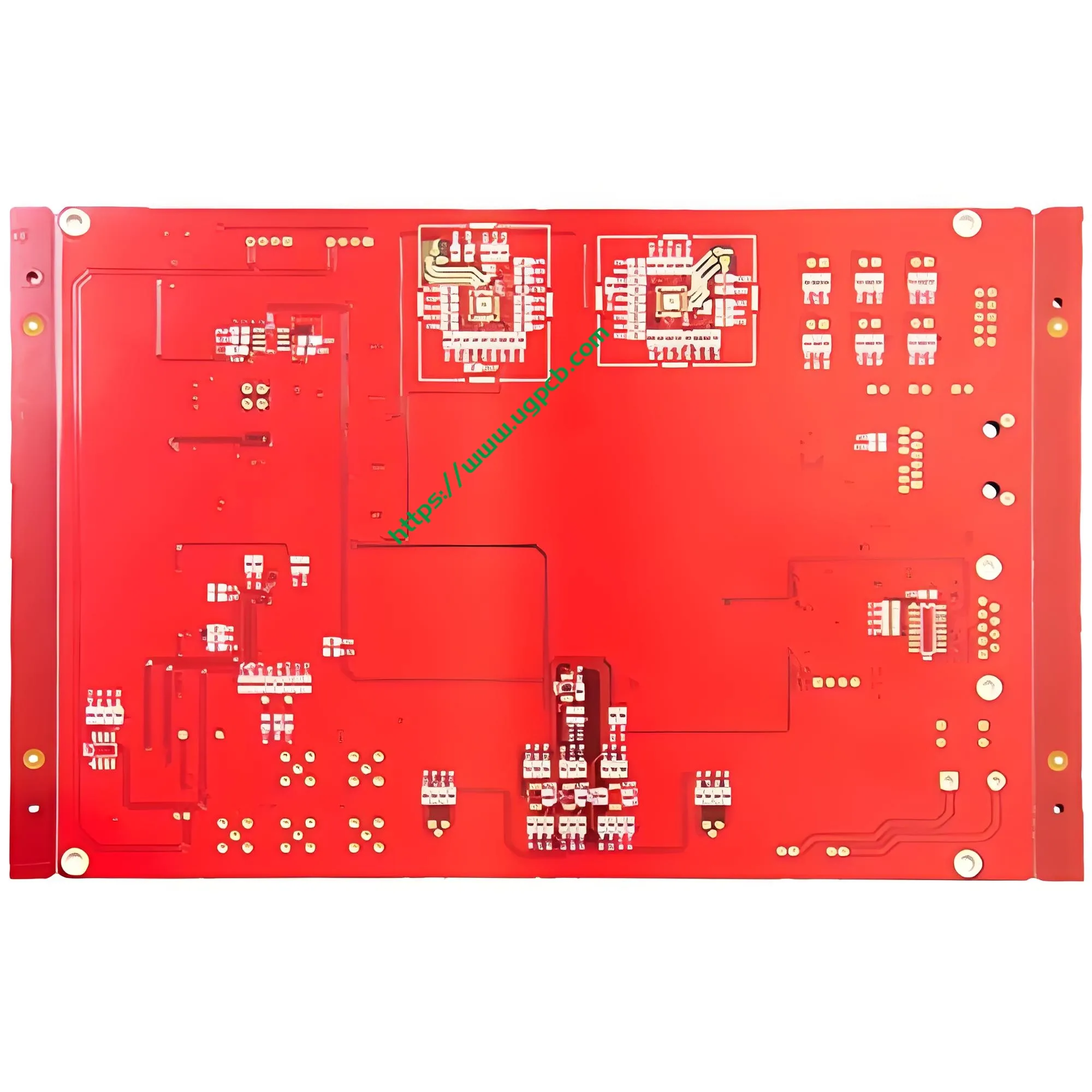
I. Product Overview: Precision PCB Engineered for Aesthetic Equipment
The laser hair removal instrument relies on a core control system. This system dictates safety, stability, and overall treatment efficacy. At the heart of this system lies the laser hair removal instrument PCB. This component is anything but trivial.
UGPCB presents a double-layer rigid printed circuit board for this exact purpose. We manufacture this board using a high-grade FR4 glass-reinforced epoxy laminate. The board thickness measures 1.0mm. Its compact dimensions are 53.68 x 37.5mm. We specifically tailor these specifications for the internal space constraints of modern portable and professional laser devices.
This PCB supports both IPL intense pulsed light and diode laser hair removal systems. It guarantees stable electrical connections and reliable signal transmission. A superior PCBA (Printed Circuit Board Assembly) forms the very foundation of high-performance aesthetic equipment. UGPCB specializes in delivering high-reliability, high-precision circuit boards to global beauty device manufacturers.
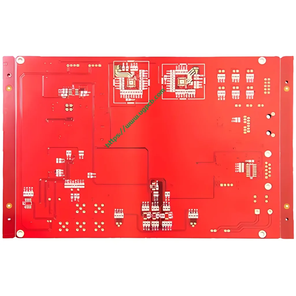
II. Product Definition: What Is a Laser Hair Removal Instrument PCB?
A laser hair removal instrument PCB is a dedicated printed circuit board. It manages core functions like power distribution, laser driver control, temperature monitoring, and user interface interaction.
Think of it as the device’s central nervous system. It accurately channels electrical energy from the battery to the laser generator. It simultaneously monitors system temperature, adjusts energy levels, and processes button inputs.
Technically, this product is a double-sided, plated-through-hole rigid PCB. It uses FR4 material. According to IPC-6012 (Qualification and Performance Specification for Rigid Printed Boards), this board fits the rigid type with plated holes. Our product meets Class 2 requirements (Dedicated Service Electronic Products). This class suits devices where high reliability is essential but not mission-critical, such as home-use and salon-grade hair removal systems.
III. Design Essentials: Engineering Precision
Excellent PCB design goes far beyond simple connectivity. Our engineering team focuses on several critical factors for this laser hair removal PCB.
3.1 Isolation and Anti-Interference Design
Laser hair removal instruments contain both high-voltage driver circuits and low-voltage control circuits. Electromagnetic interference (EMI) between these domains often causes instability. UGPCB physically isolates power and signal loops. We use a rational layer stack-up and optimized routing to mitigate mutual interference effectively.
3.2 Compact Layout and Space Optimization
The 53.68 x 37.5mm footprint demands high-density integration. Our design team achieves comprehensive functional module placement within this limited space. This dense routing ensures excellent electrical performance while enabling device miniaturization.
3.3 Thermal Management
Laser driver circuits generate considerable heat during operation. The PCB acts as a primary heat conduction path. FR4 offers inherent thermal conductivity. Combined with optimized copper pouring and thermal via placement, our design dissipates heat efficiently. This approach boosts device reliability and extends operational lifespan.
3.4 Adherence to IPC Design Standards
IPC-2221 (Generic Standard on Printed Board Design) recommends a minimum electrical clearance of 0.1mm (4 mils) for general equipment. Our design uses a line width and spacing of 0.36mm and 0.38mm. This specification far exceeds the minimum requirement. It provides a substantial safety margin for electrical performance.
IV. Working Principle: How the PCB Drives Laser Emission
The laser hair removal principle is straightforward, yet precise control requires intricate PCB coordination. The entire workflow follows these steps:
Step 1: Power Input and Management. The battery or adapter supplies raw power. The PCB’s power management circuit regulates, filters, and distributes this energy. It provides clean, stable voltage to all functional modules.
Step 2: Energy Level Control. The user selects an energy level (commonly 5 adjustable settings). The MCU (Microcontroller Unit) on the PCB receives this command. It then sends a PWM (Pulse Width Modulation) signal. This signal accurately drives the laser driver circuit, adjusting the output current to the laser generator.
Step 3: Laser Driving and Emission. The driver circuit converts electrical energy into a precise operating current for the laser diode. This current triggers the laser to emit the specific wavelength (typically 808nm or 1064nm).
Step 4: Real-Time Monitoring and Protection. Temperature sensors on the PCB continuously monitor the device’s thermal state. The MCU automatically reduces power or shuts down output if temperatures exceed safe thresholds. The PCB also handles skin-contact detection and shot-counting functions. This entire complex logic runs seamlessly on the 53.68 x 37.5mm board.
V. Primary Applications and Usage Scenarios
We design this laser hair removal PCB for diverse applications across the aesthetic industry.
| Application Field | Specific Use Case | Typical Equipment |
|---|---|---|
| Home Beauty Care | Personal hair removal | Home-use IPL devices, home laser systems |
| Professional Salons | Commercial aesthetic services | Professional-grade diode laser equipment |
| Medical Aesthetics | Clinical treatments | Medical laser therapy systems |
| ODM/OEM Manufacturing | Contract production | Branded depilatory device PCB assembly |
Furthermore, this PCB’s design logic and manufacturing processes are adaptable. They suit other aesthetic devices, including photorejuvenation machines, pigmentation removers, and RF (radio frequency) beauty instruments.
VI. Product Classification
We can scientifically classify this product across multiple dimensions:
- By Substrate Material: FR4 epoxy glass-fabric rigid PCB
- By Layer Count: 2-layer (standard double-sided rigid board)
- By Surface Finish: ENIG (Electroless Nickel Immersion Gold) / Gold-plating process
- By Flammability Rating: UL 94 V-0 flame-retardant grade
- By Application: Consumer medical / aesthetic device PCB
- By IPC-6012 Performance Level: Class 2 (Dedicated Service Electronic Products)
VII. Material Composition: FR4 Quality Assurance
7.1 FR4 Copper-Clad Laminate
We fabricate this PCB using FR4 glass-epoxy copper-clad laminate. FR4 is the predominant substrate in the PCB industry. It consists of woven glass fiber fabric impregnated with epoxy resin, cured under high heat and pressure. Per IPC-4101 (Specification for Base Materials for Rigid and Multilayer Printed Boards), FR4 exhibits these critical properties:
- Glass Transition Temperature (Tg): 130–140°C
- Dielectric Constant (Dk): 4.3–4.8 @ 1MHz
- Flammability Rating: Compliant with UL 94 V-0
- Coefficient of Thermal Expansion (CTE): 12–18 ppm/°C
Specifically, according to IPC-4101/21, standard FR-4 boards have a Tg (TMA method) ranging from 110°C to 135°C. UGPCB selects materials that comfortably exceed this baseline.
7.2 Copper Foil
UGPCB applies 35/35µm (1oz/1oz) copper foil on both sides. The 1oz specification represents the most widely used copper thickness. It strikes an optimal balance between current-carrying capacity and cost-efficiency.
7.3 Solder Mask and Legend Ink
We apply a red solder mask (red oil) combined with white silkscreen characters (white text) . This high-contrast scheme offers several advantages. It facilitates Automated Optical Inspection (AOI). It also aids manual inspection, rework, and maintenance. Furthermore, the mask protects the copper traces from oxidation, shorts, and solder bridging during assembly.
VIII. Technical Parameters and Standard Compliance
8.1 Key Parameter Summary
| Parameter | Specification | Remarks |
|---|---|---|
| Base Material | FR4 | Epoxy glass-fabric laminate |
| Board Thickness | 1.0mm | Standard rigid thickness |
| Layer Count | 2 layers | Double-sided routing |
| Dimensions | 53.68 x 37.5mm | Compact form factor |
| Minimum Aperture | 0.33mm (approx. 13 mils) | Precision drilling capability |
| Line Width / Spacing | 0.36mm / 0.38mm (14.2/15 mils) | Exceeds IPC-2221 clearance requirements |
| Copper Foil Thickness | 35/35µm (1oz/1oz) | Dual-sided heavy copper |
| Surface Finish | ENIG (Electroless Nickel Immersion Gold) | Gold plating process |
| Solder Mask Color | Red | Red oil |
| Legend Color | White | White text |
8.2 Standards Compliance
Our product design and manufacturing strictly follow these international standards:
- IPC-6012: Rigid printed board qualification and performance
- IPC-4101/21: FR-4 laminate material specification
- IPC-A-600: Acceptability of printed boards
- IPC-4552: ENIG surface finish specification
- UL 94 V-0: Highest flammability rating for plastic materials
8.3 Reliability Validation
Per IPC-6012, rigid boards must pass several quality consistency tests. UGPCB performs 100% electrical testing (flying probe or dedicated fixture testing) on every board. This process ensures flawless electrical integrity before shipment. Our boards consistently pass:
- Electrical Tests: Continuity, insulation resistance, dielectric withstand voltage
- Mechanical Tests: Peel strength, warpage, dimensional stability
- Environmental Tests: Thermal stress, temperature cycling, humidity resistance
IX. Structural Features and Physical Characteristics
9.1 Double-Layer Configuration
This 2-layer PCB features copper circuitry on both the top and bottom sides of the FR4 substrate. Plated Through-Holes (PTH) provide electrical interconnection between the layers. This structure achieves a high routing density while controlling manufacturing costs. It represents the most cost-effective PCB type for consumer electronics.
9.2 Minimum Aperture 0.33mm
The 0.33mm minimum aperture (13 mils) demonstrates UGPCB’s precision drilling capability. IPC-6012 demands tight tolerance control and adequate plating thickness within the hole wall. Our process ensures these specifications are consistently met, guaranteeing long-term reliability of the plated connections.
9.3 Line Width/Spacing Precision (0.36/0.38mm)
The 0.36mm trace width and 0.38mm clearance offer substantial electrical safety margins. Compared to the IPC-2221 baseline of 0.1mm, our design reduces crosstalk and eliminates short-circuit risks. This conservative yet precise routing enhances signal integrity in noisy high-power environments.
9.4 Advantages of the ENIG Surface Finish
We adopt Electroless Nickel Immersion Gold (ENIG) for surface treatment, fully compliant with IPC-4552. This gold plating process delivers distinct benefits:
- Superior Solderability: The gold layer protects the nickel from oxidation, guaranteeing excellent solder joint formation.
- Flat Coplanarity: ENIG provides an exceptionally smooth surface, ideal for fine-pitch component assembly.
- Extended Shelf Life: The coating resists oxidation, allowing for long-term storage without performance degradation.
- Aluminum Wire Bonding Compatibility: This finish accommodates specific high-end packaging requirements.
IPC-4552 specifies a nickel layer thickness of 3–6µm and a minimum gold layer thickness of 0.05µm. UGPCB’s ENIG process strictly adheres to these specifications.
X. Manufacturing Process Flow
Producing a high-quality laser hair removal PCB requires a rigorous, multi-step workflow. UGPCB follows this precise sequence:
- Cutting: We cut the large FR4 copper-clad panels into manageable production-sized pieces.
- Drilling: CNC drilling machines create all through-holes, including the precision 0.33mm apertures.
- Electroless Copper Deposition & Panel Plating: We chemically deposit a thin copper layer inside the holes. This process creates the conductive PTH barrel, enabling interlayer connection.
- Pattern Transfer: We laminate, expose, and develop photoresist film to transfer the circuit pattern onto the copper surfaces.
- Etching: Chemical etching removes the unwanted copper, leaving the final circuit pattern with a precise 0.36mm trace width.
- Solder Mask Application: We apply the red solder mask ink. This coating protects the circuitry and defines the exposed soldering pads.
- Surface Finish (ENIG): We apply the electroless nickel and immersion gold layers, fully compliant with IPC-4552.
- Legend Printing: We print the white silkscreen legend, clearly marking component designators and polarity indicators.
- Electrical Testing: We perform 100% flying-probe or fixture-based electrical testing to verify performance.
- Routing / V-Cutting: We route or V-cut the production panel to the final 53.68 x 37.5mm dimension.
- Final Quality Control & Packaging: We inspect the boards per IPC-A-600 criteria. Accepted boards are vacuum-packaged to protect them during shipment.
XI. Why Choose UGPCB for Your Laser Hair Removal Instrument PCB?
11.1 Authoritative Standard Endorsement
UGPCB strictly aligns with IPC-6012, IPC-4101, IPC-A-600, and IPC-4552 standards. Every process, from material selection to final inspection, follows verifiable industry benchmarks. Our quality withstands the strictest audits.
11.2 Advanced Precision Manufacturing
Our capability to produce 0.33mm minimum apertures and 0.36/0.38mm line width/spacing highlights our technical expertise. We possess the precision required for demanding laser hair removal applications.
11.3 Deep Expertise in the Aesthetic Industry
UGPCB possesses extensive domain knowledge in aesthetic device PCBs. We intimately understand the unique requirements for laser, IPL, and photorejuvenation equipment—including high-voltage isolation, thermal management, EMI suppression, and strict reliability constraints.
11.4 UL 94 V-0 Flammability Assurance
We source materials meeting the UL 94 V-0 rating—the highest flame-retardant classification. According to UL94, V-0 requires that each specimen burns for ≤10 seconds after each flame application. The total burn time for a set of five specimens must be ≤50 seconds. Furthermore, no flaming drips may ignite the underlying cotton. This ensures maximum safety, even in abnormal operating conditions.

XII. Contact Us for Your Custom PCB Solution
UGPCB provides high-quality laser hair removal instrument PCBs and turnkey PCBA services to global aesthetic device manufacturers. We are your ideal partner if you are:
- A design engineer developing next-generation hair removal systems.
- A procurement manager seeking a reliable PCB supplier.
- A product manager requiring custom PCBA solutions.
- An entrepreneurial team entering the beauty device market.
Contact us today for a product datasheet, a competitive quotation, or a free technical consultation!
📧 Email: [info@ugpcb.com]
🌐 Website: [www.ugpcb.com]
📞 Phone: [+86-135 4412 8719]
XIII. Data Source Statement
The technical standards and performance data cited in this article originate from the following authoritative institutions:
- IPC (Association Connecting Electronics Industries) — Standards referenced include IPC-6012 (Qualification and Performance Specification for Rigid Printed Boards), IPC-4101 (Specification for Base Materials for Rigid and Multilayer Printed Boards), IPC-A-600 (Acceptability of Printed Boards), IPC-2221 (Generic Standard on Printed Board Design), and IPC-4552 (Specification for Electroless Nickel/Immersion Gold (ENIG) Plating for Printed Boards).
- UL (Underwriters Laboratories) — UL 94 (Standard for Tests for Flammability of Plastic Materials for Parts in Devices and Appliances) V-0 flame rating.
- Industry Technical Publications — FR4 material property parameters (Tg 130–140°C, Dk 4.3–4.8 @ 1MHz, CTE 12–18 ppm/°C) are recognized reference values from composite material datasheets and IPC-4101 guidelines.













