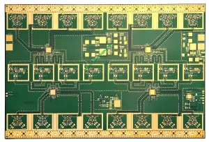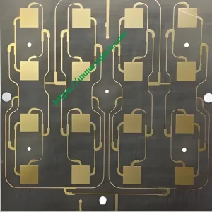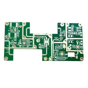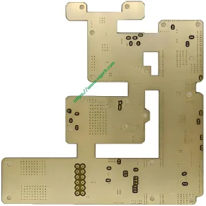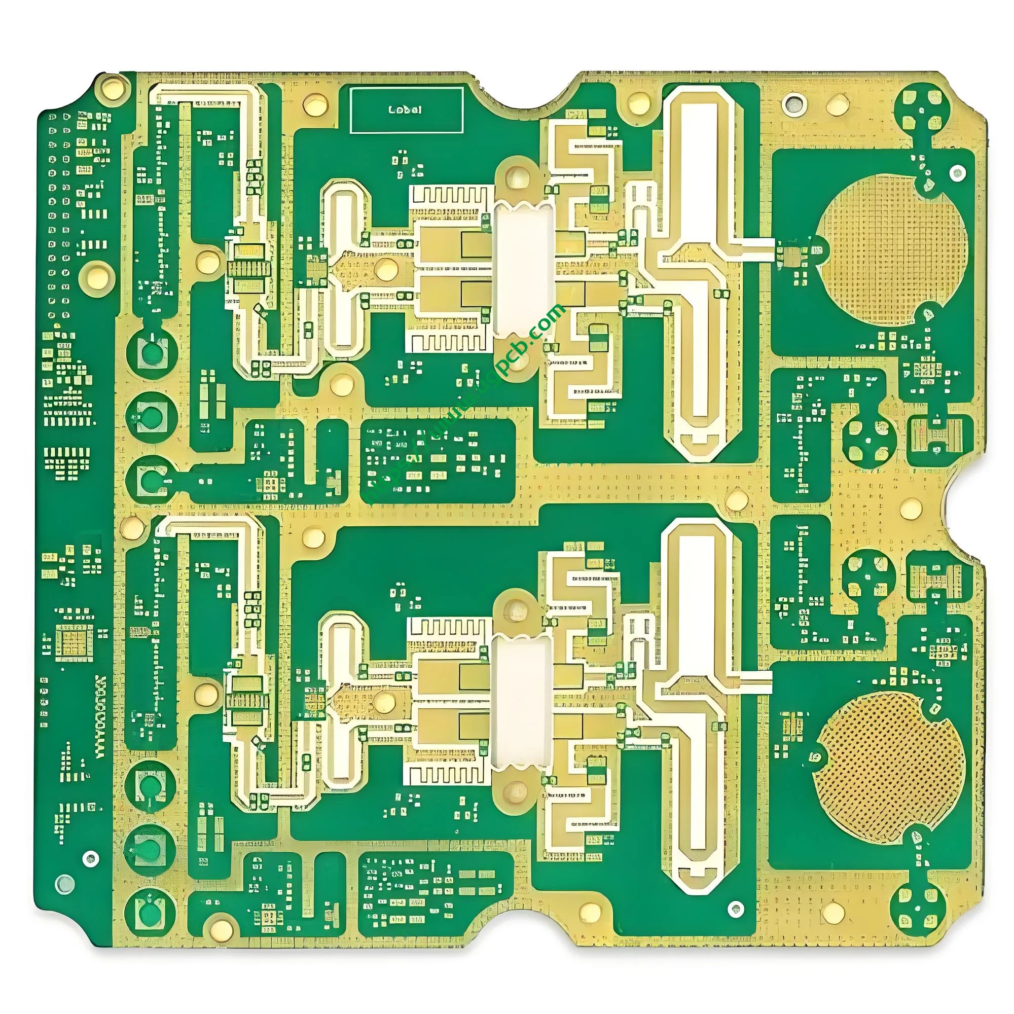
Product Overview
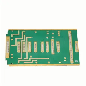
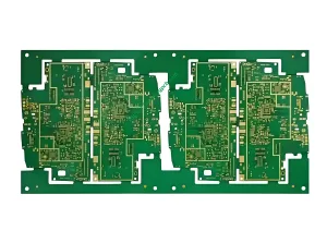
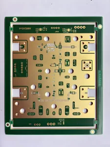
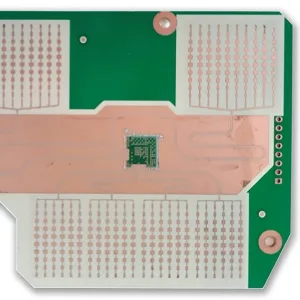
The Lightwave Communications PCB Board is a high-performance 6-layer hybrid blind buried via printed circuit board engineered by UGPCB for optical communication and high-speed digital signal transmission applications. This product features a hybrid stack-up combining TU872 high-speed digital material with Rogers RO4350B high-frequency material. The design merges high-speed digital signal processing capabilities with exceptional RF and microwave signal transmission performance. This PCB serves as an ideal interconnect solution for optical communication ground receiving equipment, high-speed optical transceivers, and base station RF front-end modules.
The PCB industry continues its push toward higher frequencies, faster speeds, and greater density. Single-material solutions can no longer meet the conflicting demands of high-speed digital signals and RF analog signals. UGPCB addresses this challenge through the TU872+RO4350B hybrid design. This 6-layer PCB achieves an optimal balance among signal integrity, thermal management, and manufacturing cost.

Product Classification
Per IPC-6012E Qualification and Performance Specification for Rigid Printed Boards, this product falls into the following categories:
| Classification Dimension | Category |
|---|---|
| Structure Type | Multilayer rigid printed board (6 layers) with blind and buried vias |
| Material System | Hybrid laminate (high-speed digital material + high-frequency material) |
| Surface Finish | Electroless Nickel/Immersion Gold (ENIG), per IPC-4552 |
| Reliability Class | Meets IPC-6012 Class 2 (dedicated service electronic products) and Class 3 (high-reliability electronic products) requirements |
| Flammability Rating | UL 94 V-0 |
| Application Domain | Optical communication / telecommunications infrastructure PCB |
Core Technical Specifications
| Parameter | Specification |
|---|---|
| Layers | 6 layers |
| Material | TU872 (high-speed digital layers) + RO4350B (high-frequency layers) |
| Board Thickness | 1.8 mm |
| Copper Thickness | 35/35/35/35 μm (uniform distribution across all layers) |
| Smallest Hole Diameter | 0.20 mm |
| Surface Treatment | ENIG (2U” gold thickness) |
| Technical Features | Vacuum plugging + Blind and buried vias |
Key Material Properties
Rogers RO4350B High-Frequency Material (for RF/microwave signal layers):
- Dielectric Constant (Dk): 3.48 ± 0.05 @ 10 GHz
- Dissipation Factor (Df): 0.0037 @ 10 GHz
- Z-axis Coefficient of Thermal Expansion (CTE): 32 ppm/°C
- Flammability Rating: UL 94 V-0
- Thermal Conductivity: 0.69 W/(m·K)
TU872 High-Speed Digital Material (for high-speed digital signal layers):
- Dielectric Constant (Dk): < 3.5 @ 10 GHz
- Dissipation Factor (Df): ~0.009 @ 10 GHz
- High glass transition temperature (Tg) with excellent thermal stability and CAF resistance
Design Guidelines
Hybrid Stack-up Architecture
This 6-layer PCB employs a hybrid stack-up with TU872 and RO4350B materials. The core design principle positions RO4350B on outer layers or specific signal layers requiring high-frequency RF signal transmission, while TU872 serves the high-speed digital signal processing layers. This strategic material allocation enables a single PCB to handle both GHz-level RF signals and high-speed digital logic signals, eliminating the performance compromises inherent in single-material solutions.
Blind and Buried Via Design
Blind vias connect outer layers to inner layers without penetrating the entire board thickness. Buried vias reside entirely within the board, invisible from either outer surface. This 6-layer PCB leverages blind and buried via technology to achieve HDI-level routing density.
Per IPC-6012E, multilayer boards with blind and buried vias must meet stringent plating and fill requirements. The 0.20 mm minimum hole diameter balances manufacturing yield with high-density routing capability. In a 6-layer board, blind vias from the outer layer to inner layers require precise depth control—they must penetrate to the target inner layer without damaging inner-layer circuits, while maintaining sufficient connection area.
Impedance Control Design
The characteristic impedance of signal transmission lines follows this formula (microstrip structure):
Where is the dielectric constant, is the dielectric thickness, is the trace width, and is the copper thickness. RO4350B’s tight Dk tolerance of ±0.05 ensures minimal deviation between designed and fabricated impedance values. This precision proves critical for accurate 50Ω single-ended or 100Ω differential impedance control in optical communication equipment.
Operating Principles
Signal Transmission Principles
At high frequencies, PCB signal transmission lines function as distributed parameter transmission lines. The dielectric constant (Dk) of the substrate material determines signal propagation velocity:
Where is the speed of light in vacuum (3×10⁸ m/s) and is the effective dielectric constant. RO4350B’s low Dk value (3.48) enables signal propagation at approximately 54% of the speed of light in vacuum—significantly faster than conventional FR-4 materials (Dk ≈ 4.2-4.8).
Loss Mechanisms
Total signal loss in PCB transmission lines consists of conductor loss and dielectric loss. Dielectric loss directly correlates with the material’s dissipation factor (Df):
Where is signal frequency and is Df. RO4350B’s Df of just 0.0037 at 10 GHz yields extremely low dielectric loss per unit length. This characteristic proves essential for optical communication signals operating at frequencies above 10 GHz.
Blind and Buried Via Electrical Connections
Blind and buried vias establish vertical interconnections between specific layers within the 6-layer PCB stack-up. Compared to through-hole vias, they significantly reduce parasitic capacitance and inductance effects that degrade high-speed signal integrity. This reduction in parasitic effects has a decisive impact on maintaining signal integrity for high-speed digital and RF signals.
Manufacturing Process
Hybrid Laminate Preparation
The TU872 and RO4350B hybrid stack-up represents the core manufacturing challenge for this product. These two materials have different CTE characteristics—RO4350B exhibits a Z-axis CTE of 32 ppm/°C, while TU872 as a modified epoxy system has different thermomechanical properties. UGPCB achieves reliable hybrid interface bonding and strength through precise lamination parameter control (temperature profile, pressure profile, and ramp rate).
Blind and Buried Via Fabrication
- Buried Via Formation: Inner-layer cores undergo drilling and copper plating before lamination, encapsulating the buried vias within the board
- Blind Via Formation: After lamination, controlled-depth drilling from the outer layer targets the specified inner layer with precise depth control
Vacuum Plugging Process
Per IPC-4761 Design Guide for Protection of Printed Board Via Structures, vacuum plugging falls under Via Protection Type VI (complete fill and cover) or Type VII (complete fill) categories. Key process parameters:
- Process Flow: Drilling → Desmear → Vacuum Plugging → Curing → Grinding
- Plug Fill Rate: ≥ 85% (per IPC-6012 requirements)
- The vacuum environment eliminates air bubbles from the via holes, ensuring complete resin fill of blind and buried vias
Surface Finish (ENIG)
Electroless Nickel/Immersion Gold (ENIG, 2U” gold thickness) surface finish complies with IPC-4552 specifications:
- Electroless Nickel Layer: 3-6 μm
- Immersion Gold Layer: ≥ 0.05 μm (2U” ≈ 0.05 μm)
- ENIG provides a flat solderable surface, excellent solderability, and long shelf life
Performance Characteristics
Signal Integrity (SI) Advantages
- Low Insertion Loss: RO4350B’s low Df (0.0037@10 GHz) minimizes high-frequency signal energy loss during transmission
- Low Dielectric Constant Variation: Dk tolerance of only ±0.05 ensures impedance consistency
- Stable Electrical Performance: TU872 maintains electrical properties across varying temperature and humidity conditions
Thermal Management Performance
- 1.8 mm board thickness provides excellent thermal mass and mechanical strength
- RO4350B thermal conductivity of 0.69 W/(m·K) effectively dissipates heat
- TU872’s high Tg ensures dimensional stability at elevated temperatures
Reliability
- Vacuum plugging ensures void-free blind and buried vias, meeting IPC-6012 Class 2/3 requirements
- Uniform 35 μm copper thickness across all four layers ensures current-carrying capacity and heat dissipation
- UL 94 V-0 flammability rating—flame extinguishes within 10 seconds after removal
Application Scenarios
Ground Receiving Equipment
This represents the primary target application for this product. Ground receiving equipment must simultaneously process high-frequency RF signals from satellites or microwave links (requiring RO4350B material) and baseband digital signal processing (requiring TU872 material). This 6-layer hybrid PCB precisely addresses this dual requirement.

Optical Communication Systems
- Fiber-optic network transmission equipment
- Optical transceivers
- Optical amplifiers
High-Speed Digital Communications
- 5G communication base station RF front-ends
- High-speed data switching equipment
- Test and measurement instruments
Why Choose UGPCB?
- Mature Hybrid Lamination Technology: Extensive production experience with TU872+RO4350B hybrid stack-ups with controllable yield
- Advanced Blind and Buried Via Capability: 0.20 mm minimum hole diameter with vacuum plugging meets HDI interconnection requirements
- End-to-End Quality Control: Full-process quality management from material receiving to finished product shipping, strictly per IPC-6012E standards
- Rapid Response: Professional engineering team provides DFM (Design for Manufacturability) review support
Inquiry Guidance
To obtain samples, volume pricing, or technical support for the Lightwave Communications PCB Board, please provide:
- Gerber files (including stack-up details)
- BOM list (if PCBA services are required)
- Special performance requirements (impedance values, test specifications, etc.)
UGPCB’s team will deliver professional technical evaluation and quotation within 24 hours.
Data Source Declaration
Technical data and standards cited in this document derive from the following authoritative sources:
- Rogers Corporation – RO4350B™ Laminate Data Sheet
- IPC (Association Connecting Electronics Industries) – IPC-6012E Qualification and Performance Specification for Rigid Printed Boards; IPC-4761 Design Guide for Protection of Printed Board Via Structures; IPC-4552 Performance Specification for Electroless Nickel/Immersion Gold (ENIG) Plating for Printed Boards
- UL (Underwriters Laboratories) – UL 94 Standard for Tests for Flammability of Plastic Materials for Parts in Devices and Appliances
- Taiyo Tech (TUC) – TU-872 SLK High-Speed Material Technical Data