
What Is a Millimeter Wave Radar PCB? — A Complete Guide to High‑Frequency Hybrid Technology
A millimeter wave radar PCB is a specialized high‑frequency printed circuit board designed for radar systems operating in the millimeter‑wave spectrum, typically at 77GHz and 79GHz. Unlike standard FR‑4 PCBs, millimeter wave radar PCBs must use high‑frequency materials with stable dielectric constants and ultra‑low loss characteristics to ensure precise target detection and reliable signal integrity at millimeter‑wave frequencies.
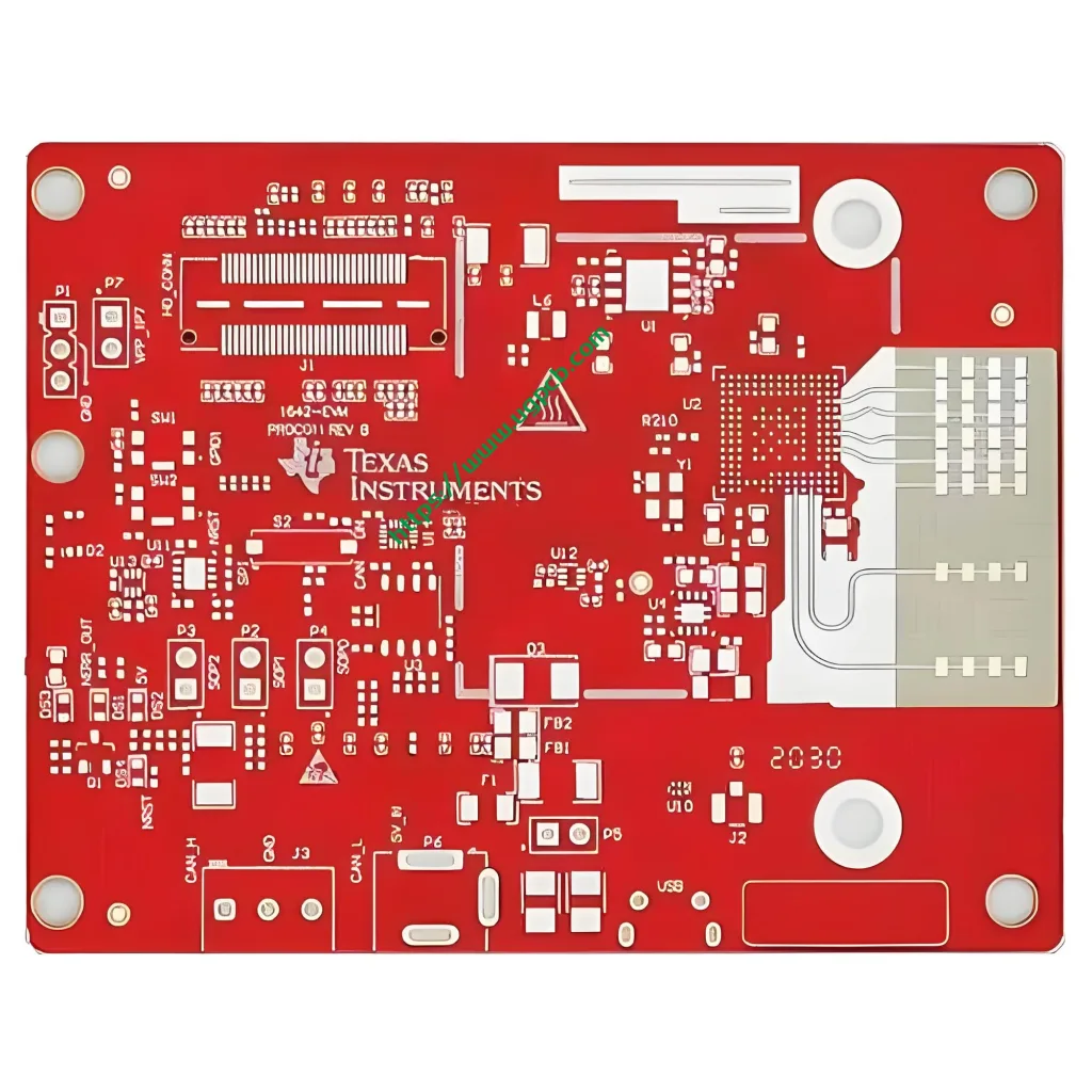
The UGPCB millimeter wave radar PCB circuit board featured in this article adopts a Rogers RO3003+370HR high‑frequency hybrid stack‑up. It is a 6‑layer board with a finished thickness of 1.2mm and 1oz copper on both inner and outer layers. This board is engineered for automotive radar (77GHz), ADAS (Advanced Driver Assistance Systems), drone collision avoidance, and industrial distance measurement applications.
1. Definition and Technical Positioning of Millimeter Wave Radar PCB
A millimeter wave radar PCB is a specialized printed circuit board that operates in the millimeter‑wave frequency range (typically 30GHz to 300GHz, with wavelengths from 1mm to 10mm). Compared to conventional PCBs, millimeter wave radar PCBs impose stringent requirements on dielectric constant stability, dissipation factor, coefficient of thermal expansion (CTE), and manufacturing precision.
From a PCB classification perspective, the millimeter wave radar PCB belongs to the High‑Frequency PCB category and can be further classified as:
- By Frequency: Millimeter‑wave band PCB (30GHz–300GHz)
- By Material: PTFE/ceramic‑filled composite high‑frequency hybrid PCB
- By Structure: 6‑layer and above multilayer hybrid PCB
- By Application: Automotive electronics PCB, ADAS‑dedicated PCB, industrial sensor PCB
- By IPC Standard: Manufactured to IPC‑6012 Class 3 high‑reliability level
This product is a millimeter wave radar PCB circuit board with a “hybrid” construction. It combines Rogers RO3003 high‑frequency material (for RF signal layers) with 370HR high‑performance epoxy material (for power and ground layers) through a lamination process. This approach ensures excellent RF signal quality while maintaining structural strength and cost‑effectiveness.
2. Design Considerations for 6‑Layer Hybrid Millimeter Wave Radar PCB
Designing a 77GHz millimeter wave radar PCB requires systematic consideration of impedance control, stack‑up configuration, signal integrity, electromagnetic compatibility (EMC), and thermal management.
2.1 Stack‑Up Design Principles
This product features a symmetrical 6‑layer stack‑up with a finished board thickness of 1.2mm. At 77GHz, the wavelength is approximately 3.9mm (calculated as λ = c/f, where c = 3×10⁸ m/s and f = 77×10⁹ Hz). At this frequency, every trace and every via on the PCB behaves as a complex component that affects RF characteristics. Key stack‑up design principles include:
- Tight coupling between signal and reference layers: The reference ground plane for RF microstrip lines must be placed immediately adjacent to the signal layer, with a spacing of 5mil (0.127mm) or less to minimize signal return path inductance.
- Symmetrical lamination: Symmetrical material distribution across the stack‑up prevents PCB warpage caused by thermal stress.
- Laser‑drilled blind vias: L1‑L2 and L3‑L6 blind via structures shorten signal paths and reduce transmission loss at millimeter‑wave frequencies.
2.2 Impedance Control and Trace Width Design
Maintaining stable 50Ω characteristic impedance is critical for signal integrity in millimeter‑wave PCB design. The microstrip line impedance can be approximated using the following empirical formula:
Where:
- W = trace width
- H = dielectric thickness
- T = copper foil thickness (1oz ≈ 35μm)
- εr = dielectric constant
This product features a trace width and spacing of 0.1mm (4mil). Combined with the 5mil RO3003 dielectric layer and a stable dielectric constant of εr = 3.0±0.04, this design achieves precise 50Ω impedance control.
2.3 Millimeter‑Wave PCB Design Guidelines
- Place RF front‑end close to the antenna: Position RF MMICs and front‑end components immediately adjacent to the antenna array. Keep 77GHz signal trace lengths under 10mm.
- Via stitching: Use dense ground via arrays (via stitching) in RF signal areas to suppress parasitic mode propagation and reduce radiation loss.
- Antenna array design: Implement microstrip patch antenna arrays (4–16 elements) to achieve narrow beamwidths of 1–3° through directional interference, meeting the angular resolution requirements for 77GHz long‑range perception.
3. Operating Principle and Technical Mechanisms of Millimeter Wave Radar PCB
3.1 Basic Operating Principle
The millimeter wave radar PCB serves as the core carrier of the radar system. Its operating principle is based on the transmission and reception of electromagnetic waves. The microstrip antenna array on the millimeter wave radar PCB transmits Frequency Modulated Continuous Wave (FMCW) signals (76GHz–81GHz). When these signals encounter a target object, they generate echoes that are captured by the receive antenna. The signal then passes through the RF front‑end, mixer, ADC conversion, and DSP digital signal processor to calculate the target’s distance, velocity, and angle.
Within this system, the millimeter wave radar PCB performs the following functions:
- Signal transmission: Transmits 77GHz RF signals with minimal insertion loss.
- Antenna radiation: Microstrip patch antenna arrays are directly integrated on the PCB for energy radiation.
- Impedance matching: Ensures 50Ω impedance consistency between the RF MMIC and the antenna.
- Power management: Provides stable power and ground return paths for the radar chipset.
- Thermal management: Conducts heat from high‑power devices to heat dissipation structures through thermal paths.
3.2 Millimeter‑Wave Signal Transmission Characteristics on PCB
At millimeter‑wave frequencies, the skin effect becomes highly significant. At 77GHz, the skin depth of copper conductors is:
Where f = 77GHz and copper conductivity σ ≈ 5.8×10⁷ S/m. Since the skin depth is far less than the 1oz copper foil thickness (35μm), current effectively flows only through an extremely thin layer on the copper surface. This is why copper surface roughness has such a critical impact on signal loss in millimeter‑wave PCBs — rough surfaces significantly increase the effective path length, resulting in higher insertion loss.
3.3 Importance of Dielectric Constant Stability
Variations in dielectric constant with temperature and frequency directly affect phase velocity, thereby altering the antenna’s beam steering angle. The RO3003 material exhibits a dielectric constant thermal coefficient of only ‑3 ppm/°C across the ‑50°C to 150°C temperature range. This represents an exceptionally high level of stability within the industry, ensuring phase stability and ranging accuracy of the radar system across the full automotive temperature range (‑40°C to +125°C).
4. Classification of Millimeter Wave Radar PCB
Millimeter wave radar PCBs can be systematically classified according to several dimensions:
4.1 By Operating Frequency Band
| Frequency Band | Wavelength | Primary Application | Typical PCB Material |
|---|---|---|---|
| 24GHz | 12.5mm | Short‑range corner radar (~60m detection) | Rogers RO4003C |
| 60GHz | 5.0mm | In‑cabin vital sign detection | Rogers RO3003 |
| 77GHz | 3.9mm | Forward long‑range main radar (~200m) | RO3003+PTFE hybrid |
| 79GHz | 3.8mm | High‑resolution imaging radar (4GHz bandwidth) | RO3003G2 |
The 77GHz and 79GHz bands have become the mainstream choice for automotive millimeter‑wave radar due to their long detection range (approximately 200m) and high resolution, making them essential perception technologies for ADAS and autonomous driving.
4.2 By Layer Count
- 4‑layer millimeter wave radar PCB: Suitable for basic corner radar and low‑power applications.
- 6‑layer millimeter wave radar PCB (this product): Balances RF performance and manufacturing cost for 77GHz main radar.
- 8–16 layer millimeter wave radar PCB: Used for integrated high‑end radar modules with multi‑channel transceiver functionality.
4.3 By Material Construction
- Single‑material millimeter wave radar PCB: Entirely composed of PTFE or ceramic‑filled high‑frequency materials.
- Hybrid millimeter wave radar PCB (this product): RO3003 high‑frequency layers + 370HR standard FR‑4 layers, balancing RF performance and structural cost.
- LTCC millimeter wave radar substrate: Low‑temperature co‑fired ceramic process for high‑end antenna integration solutions.
4.4 By Application Scenario
- Automotive 77GHz radar PCB: ACC adaptive cruise control, AEB automatic emergency braking, BSD blind spot detection.
- Industrial millimeter wave radar PCB: Liquid level measurement, security surveillance, traffic flow monitoring.
- Drone millimeter wave radar PCB: Collision avoidance, terrain following, obstacle detection systems.
- 5G millimeter wave antenna PCB: 5G backhaul links, millimeter‑wave base station antenna arrays.
5. Key Performance Parameters of RO3003+370HR High‑Frequency Hybrid PCB
5.1 Dielectric Constant (Dk)
The RO3003 high‑frequency material used in this product has a process dielectric constant of Dk = 3.00±0.04 at 10GHz (tested per IPC TM‑650 2.5.5.5). The measured dielectric constant at 77GHz is approximately 3.07. The Dk of 3.0 RO3003 material maintains exceptional stability across different temperatures and frequencies, eliminating the Dk step‑change near room temperature that is characteristic of PTFE glass materials. This makes it ideal for 77GHz automotive radar and ADAS applications.
The 370HR material has a dielectric constant of approximately 4.04 at 10GHz and is used for power and ground layers in the hybrid stack‑up.
Data Source: Dk data above sourced from Rogers Corporation official data sheets and IPC TM‑650 standard test methods.
5.2 Dissipation Factor (Df)
This product features a dissipation factor (loss tangent) of 0.001 (nominal value 0.0010@10GHz). This represents one of the lowest loss levels among commercially available high‑frequency laminates, ensuring minimal transmission loss for 77GHz millimeter‑wave signals over long distances on the PCB.
Signal attenuation on standard FR‑4 material at 77GHz can reach several dB/cm, while the ultra‑low Df of RO3003 allows signals to travel between the antenna and RF chip with minimal loss — directly determining the effective detection range of the radar.
5.3 Thermal Conductivity
The thermal conductivity of RO3003 material is 0.50 W/m·K at 50°C (ASTM D5470). The 370HR material has a thermal conductivity of approximately 0.4–4 W/m·K (depending on test direction). The overall hybrid structure has a nominal thermal conductivity of approximately 0.69 W/m·K.
Compared to standard FR‑4’s 0.3–0.5 W/m·K thermal conductivity, the 0.69 W/m·K value indicates superior heat conduction capability. In 77GHz radar modules, RF power amplifiers can dissipate several W/cm² of heat. Good thermal conductivity effectively reduces chip junction temperature and improves long‑term reliability.
5.4 Coefficient of Thermal Expansion (CTE)
The CTE values for RO3003 material are: X‑axis 17 ppm/°C, Y‑axis 16 ppm/°C, and Z‑axis 25 ppm/°C. The low and isotropic CTE characteristics ensure that the various material layers expand uniformly during reflow soldering temperature cycles (peak temperature approximately 260°C), preventing via barrel cracking or delamination.
The 370HR material also exhibits excellent thermal properties and low CTE, with a Z‑axis CTE of approximately 45 ppm/°C (below Tg), T260 > 60 minutes, and T288 > 30 minutes, demonstrating outstanding heat resistance under high‑temperature stress.
5.5 Comprehensive Performance Parameter Summary
| Parameter | Specification | Test Standard / Data Source |
|---|---|---|
| Laminate | Rogers RO3003 + 370HR | Rogers/Isola Official Data |
| Dielectric Constant (Dk) | 3.00 ±0.04 (@10GHz) | IPC TM‑650 2.5.5.5 |
| Dissipation Factor (Df) | 0.0010 (@10GHz) | Rogers Corporation Data Sheet |
| Dielectric Thickness | 5mil (0.127mm) | UGPCB Product Specification |
| Layer Count | 6 layers | Symmetrical hybrid stack‑up |
| Finished Board Thickness | 1.2mm | ±10% tolerance |
| Inner/Outer Copper Thickness | 1oz (35μm) | IPC‑6012 Class 3 Standard |
| Thermal Conductivity | 0.69 W/m·K (overall) | Hybrid composite calculation |
| Via Treatment | Resin Plug Hole (IPC‑4761 Type IV) | IPC‑4761 Via Protection Standard |
| Surface Finish | Immersion Silver (IPC‑4553) | IPC‑4553 Specification |
| Flammability Rating | UL94 V‑0 | UL Standard |
| Glass Transition Temperature (Tg) | 180°C (370HR) | DSC Testing |
| Water Absorption | 0.04% | D48/50% Method |
6. Structure and Stack‑Up Design of Millimeter Wave Radar PCB
6.1 6‑Layer Hybrid Stack‑Up Configuration
This product features a symmetrical 6‑layer hybrid structure combining Rogers RO3003 and 370HR:
| Layer | Material / Function | Key Parameters |
|---|---|---|
| L1 (Top) | RO3003 + 1oz copper | RF microstrip antenna / signal layer |
| L2 (Inner) | Prepreg + 1oz copper | Reference ground plane (tightly coupled) |
| L3 (Inner) | 370HR + 1oz copper | Power layer / low‑speed signal layer |
| L4 (Inner) | 370HR + 1oz copper | Ground layer / return plane |
| L5 (Inner) | Prepreg + 1oz copper | Signal layer / shielding layer |
| L6 (Bottom) | RO3003 + 1oz copper | RF signal layer / auxiliary antenna layer |
Design Rationale: RO3003 is used exclusively in the high‑frequency signal regions (L1‑L2 and L5‑L6), while 370HR is used for the middle power and ground layers. This hybrid layout ensures RF performance while leveraging 370HR’s high Tg, low CTE, and superior mechanical strength — significantly reducing overall material cost.
6.2 Via Structure: Resin Plug Hole Process (IPC‑4761 Type IV)
This product employs the Resin Plug Hole (IPC‑4761 Type IV) via protection process. Specifically, vias are first partially filled with non‑conductive epoxy resin (plugging) and then covered with solder mask over the plugging material (covered).
The resin plug hole process is critical for millimeter wave radar PCBs:
- Prevents solder wicking: During reflow soldering, molten solder can be drawn into vias by capillary action, leaving insufficient solder on component pads and causing weak joints or open circuits. Resin plugging effectively prevents this “solder theft” phenomenon.
- Enhances reliability: Via structures protected by resin show significantly improved resistance to thermal cycling and mechanical vibration.
- Supports high‑density design: Resin plugging allows vias to be placed under component pads (via‑in‑pad), enabling more compact RF front‑end layouts.
- Meets IPC‑4761 standards: Type IV level via protection is a standard requirement for IPC‑6012 Class 3 high‑reliability PCBs.
6.3 Immersion Silver Surface Finish (IPC‑4553)
The surface finish is Immersion Silver (IPC‑4553) , which deposits a uniform thin silver layer (0.1–0.4μm) on the copper surface to protect against oxidation and ensure solderability.
Reasons for choosing immersion silver over other surface finishes:
- Superior RF performance: Silver has the highest electrical conductivity among all metals (≈63×10⁶ S/m), resulting in minimal conductive loss at millimeter‑wave frequencies.
- Flat surface: The immersion silver layer is extremely thin and flat, without the irregular solder bumps characteristic of HASL.
- Good solderability: Meets J‑STD‑003 standards, providing a normal storage life of 12 months or more.
- Lead‑free compatible: Fully compatible with lead‑free reflow soldering processes.
Application Note: IPC‑4553 specifies that for Class 3 high‑reliability applications in the IPC‑6010 series where no downtime is permitted (such as life support equipment and critical weapons systems), immersion silver is not currently recommended. For these applications, ENIG or ENEPIG should be specified. This product is primarily used in automotive radar applications (high‑performance electronics, not life support systems), where immersion silver achieves an optimal balance of cost and performance.
7. Manufacturing Process Flow for Millimeter Wave Radar PCB
7.1 High‑Frequency Hybrid PCB Manufacturing Flowchart
7.2 Key Manufacturing Steps
① Material Preparation and Incoming Inspection – Inspect incoming RO3003 high‑frequency laminates and 370HR laminates for Dk/Df consistency, thickness tolerance, and surface quality.
② Inner Layer Pattern Transfer – Apply photosensitive dry film to the cleaned copper surface. Transfer the circuit pattern to the copper through photolithography. Develop, etch, and strip the film to form inner layer circuit patterns.
③ Brown Oxide Treatment – Micro‑rough the inner layer copper surface to enhance adhesion between the copper and prepreg resin during lamination.
④ Hybrid Lamination – Laminate the RO3003 substrate, prepreg, and 370HR substrate under high temperature and pressure. This is the most challenging step in hybrid technology — the CTE differences and thermal expansion characteristics of the two materials must be precisely matched in lamination parameters to prevent delamination or warpage.
⑤ Laser Drilling and Mechanical Drilling – Use CO₂ lasers to drill blind vias (L1‑L2 and L3‑L6 layers) and mechanical drilling for through‑holes.
⑥ Resin Plug Hole – After drilling, use vacuum injection to fill vias with epoxy resin. Cure at high temperature, then grind the surface flat.
⑦ Outer Layer Pattern Transfer – After resin plugging, fabricate outer layer circuits through photolithography, development, etching, and film stripping.
⑧ Solder Mask Application – Apply photosensitive solder mask ink evenly across the board surface. Expose and develop to expose pads requiring soldering while covering areas that do not require soldering.
⑨ Immersion Silver Plating – Perform immersion silver treatment after solder mask application. Immerse the PCB in a silver‑ion‑containing chemical solution to deposit a uniform 0.1–0.4μm silver layer on the copper surface through displacement reaction.
⑩ Profiling – Use CNC routing to mill the circuit board to the finished outline per design drawings. Complete V‑CUT scoring for panel separation.
⑪ Electrical Testing and Reliability Inspection – Perform 100% flying probe testing (electrical continuity and isolation testing) and impedance testing. Conduct micro‑section analysis per IPC‑6012 Class 3 standards. Perform thermal stress testing (288°C/10 second solder dip) and thermal cycling reliability verification on sample boards.
8. Application Scenarios for Millimeter Wave Radar PCB
8.1 Automotive Electronics — The Core Driving Market
The automotive sector represents the largest market for millimeter wave radar PCBs. 77GHz millimeter wave radar PCBs are widely used in:
- ACC Adaptive Cruise Control: Forward long‑range radar (~200m detection distance) maintaining safe following distance.
- AEB Automatic Emergency Braking: Continuously monitors forward obstacles and automatically initiates braking when collision risk is detected.
- BSD Blind Spot Detection: Mounted on rear bumpers to monitor vehicles in blind spots.
- LCA Lane Change Assist: Monitors rapidly approaching vehicles in adjacent lanes from behind.
- Parking Assist Radar (24GHz or 77GHz) : Environment perception module for automated parking systems.
8.2 Industrial Automation and Security
- Industrial millimeter wave radar sensors: Liquid level measurement, material level detection, distance measurement.
- Smart security and perimeter protection: Personnel intrusion detection, area security monitoring.
- Traffic flow monitoring radar: Vehicle counting, speed detection, traffic violation enforcement.
8.3 Drones and Robotics
- Drone millimeter wave collision avoidance radar: Autonomous obstacle avoidance, terrain following, and altitude detection in complex environments.
- AGV automated guided vehicle navigation: Position perception and path planning for warehouse robots and industrial AGVs.
8.4 5G Communications and Millimeter‑Wave Infrastructure
- 5G millimeter‑wave backhaul link antenna PCB: High‑bandwidth communication links between base stations.
- Small cell millimeter‑wave antenna array PCB: 5G coverage in urban hotspots.
8.5 Medical and Vital Sign Monitoring
- 60GHz non‑contact vital sign detection radar PCB: In‑cabin vital sign detection, infant monitoring, and fall detection for the elderly.
9. Material Selection and Rationale for Millimeter Wave Radar PCB
9.1 RO3003 High‑Frequency Material Characteristics
RO3003 is a ceramic‑filled PTFE composite material manufactured by Rogers Corporation. It is one of the most widely used high‑frequency laminates in the 77GHz millimeter‑wave radar industry today.
Core Advantages:
- Exceptionally wideband Dk stability: Dk = 3.00±0.04, variation from 10GHz to 77GHz is less than 2.5% — far superior to standard FR‑4 (which can drift more than 15% above 10GHz).
- Ultra‑low loss: Df = 0.001@10GHz — one of the lowest‑loss commercially available PTFE‑based materials.
- Superior thermal stability: CTE closely matches that of copper (17 ppm/°C), significantly reducing thermal stress risk.
- Low water absorption: Only 0.04%, ensuring dielectric stability in humid environments.
- UL94 V‑0 flammability rating: Meets stringent flammability requirements for automotive electronics.
9.2 370HR FR‑4 Material as Complementary Layer
The 370HR material serves structural and functional roles in the non‑RF regions (power and ground layers) of the multilayer board. It is a 180°C Tg high‑performance FR‑4 system with excellent thermal properties and CAF resistance. In the hybrid stack‑up, 370HR contributes:
- High Tg (180°C): Maintains mechanical rigidity through multiple reflow cycles, resisting thermal stress deformation.
- High Td (340°C): Maintains chemical stability under extreme high temperatures.
- Superior CAF resistance: Prevents conductive anodic filament growth that can cause interlayer short circuits.
- High cost‑effectiveness: Significantly reduces the amount of high‑frequency material used, optimizing overall cost.
9.3 Advantages of Hybrid Technology
| Dimension | Full RO3003 | Full 370HR | RO3003+370HR Hybrid (This Product) |
|---|---|---|---|
| RF Performance | Excellent | Poor | Excellent |
| Structural Strength | Fair | Good | Excellent |
| Material Cost | Very High | Low | Medium |
| Manufacturing Difficulty | High | Low | Medium |
| Overall Value | Low | RF‑only applications | High |
9.4 Why FR‑4 Cannot Be Used for Millimeter‑Wave Radar
Standard FR‑4 is completely unsuitable for the 77GHz band for several reasons:
- Dielectric constant varies dramatically with frequency and temperature, causing impedance instability and phase drift.
- Dissipation factor of approximately 0.020 (@1GHz) is 20 times higher than RO3003, causing severe signal attenuation.
- Glass weave construction produces significant weave effect at millimeter‑wave frequencies, destroying transmission line uniformity.
Millimeter wave radar PCBs must use high‑frequency material systems based on PTFE/ceramic fillers.
10. Core Advantages and Differentiators of Millimeter Wave Radar PCB
10.1 Technical Advantages
1. Industry‑leading Dk stability – Across the ‑50°C to 150°C temperature range, dielectric constant variation is only ‑3 ppm/°C. Under extreme automotive temperature conditions (‑40°C to +125°C), the radar’s beam steering angle and ranging accuracy remain stable.
2. Ultra‑low transmission loss at 77GHz – With Df = 0.001@10GHz, 77GHz signal transmission loss on the millimeter wave radar PCB is below 0.1dB/cm, effectively ensuring radar detection range of 200m or more.
3. Precise impedance control – ±8% characteristic impedance control tolerance ensures 77GHz RF chain integrity and antenna efficiency.
4. High‑reliability thermal management – 0.69 W/m·K overall thermal conductivity combined with resin plug hole via structures effectively conducts heat from RF power amplifiers to heat dissipation interfaces.
5. Excellent thermal resistance – Tg ≥ 180°C and Td ≥ 340°C fully meet lead‑free reflow soldering process requirements (peak 260°C, multiple cycles).
10.2 Quality and Compliance Advantages
- IPC‑6012 Class 3 high‑reliability level manufacturing: Meets the highest level of quality and performance standards.
- UL94 V‑0 flammability certification: Meets mandatory flammability requirements for automotive and industrial equipment.
- RoHS compliant: Lead‑free, environmentally friendly manufacturing, meeting global environmental regulations.
- ISO 9001 certification: Standardized quality management system ensuring batch‑to‑batch consistency.
11. Industry Standards and Data Sources
The design, manufacturing, and quality inspection of this product strictly adhere to the following authoritative standards:
11.1 PCB Material Standards
| Standard | Title | Application |
|---|---|---|
| IPC‑4101E | Specification for Base Materials for Rigid and Multilayer Printed Boards | 370HR meets Type/127, /128, /130 |
| IPC TM‑650 2.5.5.5 | Test Methods Manual — Dielectric Constant and Dissipation Factor | Dk/Df test method |
| ASTM D5470 | Standard Test Method for Thermal Transmission Properties | Thermal conductivity test method |
11.2 PCB Process and Performance Standards
| Standard | Title | Application |
|---|---|---|
| IPC‑6012 | Qualification and Performance Specification for Rigid Printed Boards | Class 3 high‑reliability level |
| IPC‑A‑600 | Acceptability of Printed Boards | Visual and quality inspection |
| IPC‑4761 | Design Guide for Protection of Printed Board Via Structures | Via protection Type IV |
| IPC‑4553 | Specification for Immersion Silver Plating for Printed Boards | Immersion silver surface finish |
11.3 Material Safety and Reliability Standards
| Standard | Title | Application |
|---|---|---|
| UL94 V‑0 | Standard for Tests for Flammability of Plastic Materials | Flammability rating certification |
| J‑STD‑003 | Solderability Tests for Printed Boards | Solderability test standard |
| AEC‑Q100 | Failure Mechanism Based Stress Test Qualification for Integrated Circuits | Automotive‑grade component reliability |
11.4 Key Data Source Summary
- RO3003 Dk = 3.00±0.04, Df = 0.001@10GHz — Rogers Corporation Official Data Sheet
- RO3003 Dk ≈ 3.07 at 77GHz — IPCB measured data (microstrip differential phase method)
- RO3003 thermal conductivity 0.50 W/m·K (50°C, ASTM D5470) — Rogers Corporation Official Data Sheet
- 370HR Tg = 180°C, Td = 340°C, Z‑axis CTE = 45 ppm/°C — Isola 370HR Official Technical Data
- Standard FR‑4 thermal conductivity 0.3–0.5 W/m·K — Cadence PCB Substrates Technical White Paper
- 77GHz wavelength ≈ 3.9mm — Calculated from λ = c/f (c = 3×10⁸ m/s, f = 77×10⁹ Hz)
12. Why Choose UGPCB for Your Millimeter Wave Radar PCB?
12.1 UGPCB Core Capabilities
- Extensive high‑frequency hybrid experience: UGPCB has accumulated rich process experience in high‑frequency material hybrid lamination, handling everything from RO3003+370HR to more advanced material combinations.
- Precision impedance control capability: ±8% impedance control tolerance meets the demanding requirements of 77GHz RF design.
- End‑to‑end quality management: Manufacturing to IPC‑6012 Class 3 standards with rigorous quality monitoring at every production step.
- Responsive technical support: Complete engineering services from stack‑up design consultation and DFM manufacturability review to prototype fabrication.
12.2 Applicable Product Portfolio
UGPCB provides rapid prototyping and volume production services for the following millimeter wave radar PCBs:
- 77GHz automotive millimeter wave radar PCB (ACC/AEB/BSD)
- 79GHz high‑resolution imaging radar PCB
- 24GHz blind spot monitoring corner radar PCB
- 60GHz vital sign detection radar PCB
- Millimeter wave radar PCBA assemblies (compatible with TI IWR series, NXP, Infineon radar chips)
12.3 Quick Quote and Service Inquiry
| Item | Details |
|---|---|
| Product Name | 6‑Layer Rogers RO3003+370HR Millimeter Wave Radar PCB Circuit Board |
| Standard Lead Time | Prototype: 7–10 working days; Volume: 10–15 working days |
| File Formats | Gerber RS‑274X, ODB++, PCB design source files |
| Quality Assurance | 100% flying probe testing, 100% impedance testing, inspection report provided |
Millimeter Wave Radar PCB Circuit Board — Specification Summary
| Parameter | Specification |
|---|---|
| Product Name | 6‑Layer Millimeter Wave Radar PCB Circuit Board |
| Laminate | Rogers RO3003 + 370HR Hybrid |
| Dielectric Constant (Dk) | 3.0 ±0.04 (RO3003 @10GHz) |
| Dielectric Thickness | 5mil (0.127mm) |
| Layer Count | 6 layers |
| Finished Board Thickness | 1.2mm |
| Inner/Outer Copper Thickness | 1oz (35μm) |
| Minimum Trace Width/Spacing | 0.1mm / 0.1mm |
| Via Treatment | Resin Plug Hole (IPC‑4761 Type IV) |
| Surface Finish | Immersion Silver (IPC‑4553) |
| Thermal Conductivity | 0.69 W/m·K (overall) |
| Dissipation Factor | 0.001 (@10GHz) |
| Flammability Rating | UL94 V‑0 |
| Blind Via Structure | L1‑L2, L3‑L6 |
| Quality Standard | IPC‑6012 Class 3 |
| Primary Applications | 77GHz Automotive Radar, ADAS, Industrial Ranging |
Request a Quote — Get Your Custom Millimeter Wave Radar PCB Solution Today
UGPCB is committed to providing high‑quality high‑frequency hybrid millimeter wave radar PCB solutions to customers worldwide. Whether you are prototyping a 77GHz automotive radar or need volume production of millimeter wave radar PCBs, our engineering team is ready to provide professional technical support and service.
Contact UGPCB Today:
- Send Gerber files to: [sales@ugpcb.com]
- Visit our website: [www.ugpcb.com]
Please provide the following information for a quick quote:
- Gerber files or PCB design drawings
- Quantity required (prototype / small batch / volume production)
- Target application (e.g., 77GHz automotive radar, industrial detection, etc.)
- Special requirements (lead‑free requirements, specific testing needs, etc.)


